- 您現在的位置:買賣IC網 > PDF目錄373913 > AD7676ASTRL (ANALOG DEVICES INC) 16-Bit +-1 LSB INL, 500 kSPS, Differential ADC PDF資料下載
參數資料
| 型號: | AD7676ASTRL |
| 廠商: | ANALOG DEVICES INC |
| 元件分類: | ADC |
| 英文描述: | 16-Bit +-1 LSB INL, 500 kSPS, Differential ADC |
| 中文描述: | 1-CH 16-BIT SUCCESSIVE APPROXIMATION ADC, SERIAL/PARALLEL ACCESS, PQFP48 |
| 封裝: | 1.40 MM HEIGHT, PLASTIC, MS-026BBC, LQFP-48 |
| 文件頁數: | 14/20頁 |
| 文件大小: | 321K |
| 代理商: | AD7676ASTRL |
REV. 0
AD7676
–
14
–
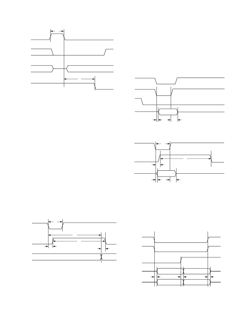
t
9
RESET
DATA
BUSY
CNVST
t
8
Figure 12. RESET Timing
For other applications, conversions can be automatically initi-
ated. If
CNVST
is held low when BUSY is low, the AD7676
controls the acquisition phase and then automatically initiates a
new conversion. By keeping
CNVST
low, the AD7676 keeps
the conversion process running by itself. It should be noted that
the analog input has to be settled when BUSY goes low. Also, at
power-up,
CNVST
should be brought low once to initiate the
conversion process. In this mode, the AD7676 could sometimes
run slightly faster than the guaranteed limit of 500 kSPS.
DIGITAL INTERFACE
The AD7676 has a versatile digital interface; it can be interfaced
with the host system by using either a serial or parallel interface.
The serial interface is multiplexed on the parallel data bus. The
AD7676 digital interface also accommodates both 3 V or 5 V
logic by simply connecting the OVDD supply pin of the AD7676
to the host system interface digital supply. Finally, by using the
OB/
2C
input pin, either two’s complement or straight binary
coding can be used.
The two signals
CS
and
RD
control the interface. When at least
one of these signals is high, the interface outputs are in high
impedance. Usually,
CS
allows the selection of each AD7676 in
multi-circuits applications and is held low in a single AD7676
design.
RD
is generally used to enable the conversion result on
the data bus.
CNVST
BUSY
DATA
BUS
CS
=
RD
= 0
PREVIOUS CONVERSION DATA
NEW DATA
t
1
t
10
t
4
t
3
t
11
Figure 13. Master Parallel Data Timing for Reading
(Continuous Read)
PARALLEL INTERFACE
The AD7676 is configured to use the parallel interface (Figure 13)
when the SER/
PAR
is held low. The data can be read either
after each conversion, which is during the next acquisition
phase, or during the following conversion as shown, respectively,
in Figure 14 and Figure 15. When the data is read during the
conversion, however, it is recommended that it be read-only
during the first half of the conversion phase. That avoids any
potential feedthrough between voltage transients on the digital
interface and the most critical analog conversion circuitry.
DATA
BUS
t
12
t
13
BUSY
CS
RD
CURRENT
CONVERSION
Figure 14. Slave Parallel Data Timing for Reading
(Read after Convert)
CS
= 0
CNVST
,
RD
t
1
PREVIOUS
CONVERSION
DATA
BUS
t
12
t
13
BUSY
t
4
t
3
Figure 15. Slave Parallel Data Timing for Reading (Read
During Convert)
The BYTESWAP pin allows a glueless interface to an 8-bit bus.
As shown in Figure 16, the LSB byte is output on D[7:0] and
the MSB is output on D[15:8] when BYTESWAP is low. When
BYTESWAP is high, the LSB and MSB bytes are swapped and
the LSB is output on D[15:8] and the MSB is output on D[7:0].
By connecting BYTESWAP to an address line, the 16-bit data
can be read in two bytes on either D[15:8] or D[7:0].
CS
RD
BYTE
PINS D[15:8]
PINS D[7:0]
HI-Z
HI-Z
HIGH BYTE
LOW BYTE
LOW BYTE
HIGH BYTE
HI-Z
HI-Z
t
12
t
12
t
13
Figure 16. 8-Bit Parallel Interface
相關PDF資料 |
PDF描述 |
|---|---|
| AD7677 | 16-Bit, 1 LSB INL, 1 MSPS Differential ADC |
| AD7677AST | 16-Bit, 1 LSB INL, 1 MSPS Differential ADC |
| AD7677ASTRL | 16-Bit, 1 LSB INL, 1 MSPS Differential ADC |
| AD7679CB1 | 18-Bit, 2.5 LSB INL, 570 kSPS SAR ADC |
| AD7694 | 16-Bit, 250 kSPS PulSAR ADC in MSOP |
相關代理商/技術參數 |
參數描述 |
|---|---|
| AD7676ASTZ | 功能描述:IC ADC 16BIT 500KSPS DIFF 48LQFP RoHS:是 類別:集成電路 (IC) >> 數據采集 - 模數轉換器 系列:PulSAR® 標準包裝:1 系列:microPOWER™ 位數:8 采樣率(每秒):1M 數據接口:串行,SPI? 轉換器數目:1 功率耗散(最大):- 電壓電源:模擬和數字 工作溫度:-40°C ~ 125°C 安裝類型:表面貼裝 封裝/外殼:24-VFQFN 裸露焊盤 供應商設備封裝:24-VQFN 裸露焊盤(4x4) 包裝:Digi-Reel® 輸入數目和類型:8 個單端,單極 產品目錄頁面:892 (CN2011-ZH PDF) 其它名稱:296-25851-6 |
| AD7676ASTZKL1 | 制造商:Rochester Electronics LLC 功能描述: 制造商:Analog Devices 功能描述: |
| AD7676ASTZRL | 功能描述:IC ADC 16BIT DIFF INP 48LQFP RoHS:是 類別:集成電路 (IC) >> 數據采集 - 模數轉換器 系列:PulSAR® 標準包裝:1 系列:- 位數:14 采樣率(每秒):83k 數據接口:串行,并聯 轉換器數目:1 功率耗散(最大):95mW 電壓電源:雙 ± 工作溫度:0°C ~ 70°C 安裝類型:通孔 封裝/外殼:28-DIP(0.600",15.24mm) 供應商設備封裝:28-PDIP 包裝:管件 輸入數目和類型:1 個單端,雙極 |
| AD7677 | 制造商:AD 制造商全稱:Analog Devices 功能描述:18-Bit, 2.5 LSB INL, 570 kSPS SAR ADC |
| AD7677AAST | 制造商:Analog Devices 功能描述: |
發布緊急采購,3分鐘左右您將得到回復。