- 您現在的位置:買賣IC網 > PDF目錄373913 > AD7677 (Analog Devices, Inc.) 16-Bit, 1 LSB INL, 1 MSPS Differential ADC PDF資料下載
參數資料
| 型號: | AD7677 |
| 廠商: | Analog Devices, Inc. |
| 英文描述: | 16-Bit, 1 LSB INL, 1 MSPS Differential ADC |
| 中文描述: | 16位,1 LSB INL和1 MSPS的差分ADC |
| 文件頁數: | 18/20頁 |
| 文件大小: | 322K |
| 代理商: | AD7677 |
REV. 0
AD7677
–18–
an improper bit decision made during the first half of the conver-
sion phase. For this reason, it is recommended that when an
external clock is being provided, it is a discontinuous clock that is
toggling only when BUSY is low or, more importantly, that it does
not transition during the latter half of BUSY high.
External Discontinuous Clock Data Read after Conversion
This mode is the most recommended of the serial slave modes.
Figure 19 shows the detailed timing diagrams of this method.
After a conversion is complete, indicated by BUSY returning
low, the result of this conversion can be read while both
CS
and
RD
are low. The data is shifted out, MSB first, with 16 clock
pulses and is valid on both rising and falling edge of the clock.
Among the advantages of this method, the conversion perfor-
mance is not degraded because there is no voltage transients on
the digital interface during the conversion process.
Another advantage is to be able to read the data at any speed up
to 40 MHz which accommodates both slow digital host interface
and the fastest serial reading.
Finally, in this mode only, the AD7677 provides a “daisy chain”
feature using the RDC/SDIN input pin for cascading multiple
converters together. This feature is useful for reducing compo-
nent count and wiring connections when it is desired as it is, for
instance, in isolated multiconverters applications.
An example of the concatenation of two devices is shown in
Figure 21. Simultaneous sampling is possible by using a common
CNVST
signal. It should be noted that the RDC/SDIN input is
latched on the opposite edge of SCLK of the one used to shift
out the data on SDOUT. Hence, the MSB of the “upstream”
converter just follows the LSB of the “downstream” converter
on the next SCLK cycle.
BUSY
BUSY
AD7677
#2 (UPSTREAM)
AD7677
#1 (DOWNSTREAM)
RDC/SDIN
SDOUT
CNVST
CS
SCLK
RDC/SDIN
SDOUT
CNVST
CS
SCLK
DATA
OUT
SCLK IN
CS IN
CNVST IN
BUSY
OUT
Figure 21. Two AD7677s in a “Daisy Chain” Configuration
External Clock Data Read During Conversion
Figure 20 shows the detailed timing diagrams of this method.
During a conversion, while both CS and RD are low, the result
of the previous conversion can be read. The data is shifted out,
MSB first, with 16 clock pulses, and is valid on both rising and
falling edges of the clock. The 16 bits have to be read before the
current conversion is complete. If that is not done, RDERROR
is pulsed high and can be used to interrupt the host interface
to prevent incomplete data reading. There is no “daisy chain”
feature in this mode, and RDC/SDIN input should always be
tied either high or low.
To reduce performance degradation due to digital activity, a fast
discontinuous clock of at least 25 MHz, when impulse mode is
used, 32 MHz when normal, or 40 MHz when warp mode is
used, is recommended to ensure that all the bits are read during
the first half of the conversion phase. It is also possible to begin
to read the data after conversion and continue to read the last
bits even after a new conversion has been initiated. That allows
the use of a slower clock speed like 18 MHz in impulse mode,
21 MHz in normal mode, and 26 MHz in warp mode.
MICROPROCESSOR INTERFACING
The AD7677 is ideally suited for traditional dc measurement
applications supporting a microprocessor and ac signal process-
ing applications interfacing to a digital signal processor. The
AD7677 is designed to interface either with a parallel 8-bit or
16-bit wide interface or with a general purpose serial port or I/O
ports on a microcontroller. A variety of external buffers can be
used with the AD7677 to prevent digital noise from coupling into
the ADC. The following sections illustrate the use of the AD7677
with an SPI equipped microcontroller, the ADSP-21065L and
ADSP-218x signal processors.
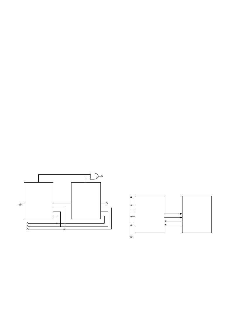
SPI Interface (MC68HC11)
Figure 22 shows an interface diagram between the AD7677 and
an SPI-equipped microcontroller like the MC68HC11. To
accommodate the slower speed of the microcontroller, the
AD7677 acts as a slave device and data must be read after
conversion. This mode also allows the “daisy chain” feature. The
convert command could be initiated in response to an internal
timer interrupt. The reading of output data, one byte at a time, if
necessary, could be initiated in response to the end-of-conversion
signal (BUSY going low) using an interrupt line of the microcon-
troller. The Serial Peripheral Interface (SPI) on the MC68HC11
is configured for master mode (MSTR) = 1, Clock Polarity Bit
(CPOL) = 0, Clock Phase Bit (CPHA) = 1, and SPI interrupt
enable (SPIE) = 1 by writing to the SPI Control Register (SPCR).
The IRQ is configured for edge-sensitive-only operation (IRQE = 1
in OPTION register).
AD7677
*
MC68HC11
*
SER/
PAR
EXT/
INT
CS
RD
IRQ
MISO/SDI
SCK
I/O PORT
BUSY
SDOUT
SCLK
CNVST
INVSCLK
DVDD
*
ADDITIONAL PINS OMITTED FOR CLARITY
Figure 22. Interfacing the AD7677 to SPI Interface
ADSP-21065L in Master Serial Interface
As shown in Figure 23, the AD7677 can be interfaced to the
ADSP-21065L using the serial interface in master mode with-
out any glue logic required. This mode combines the advantages
of reducing the wire connections and the ability to read the data
during or after conversion maximum speed transfer (DIVSCLK
[0:1] both low).
相關PDF資料 |
PDF描述 |
|---|---|
| AD7677AST | 16-Bit, 1 LSB INL, 1 MSPS Differential ADC |
| AD7677ASTRL | 16-Bit, 1 LSB INL, 1 MSPS Differential ADC |
| AD7679CB1 | 18-Bit, 2.5 LSB INL, 570 kSPS SAR ADC |
| AD7694 | 16-Bit, 250 kSPS PulSAR ADC in MSOP |
| AD7694ARM | 16-Bit, 250 kSPS PulSAR ADC in MSOP |
相關代理商/技術參數 |
參數描述 |
|---|---|
| AD7677AAST | 制造商:Analog Devices 功能描述: |
| AD7677ACP | 制造商:Analog Devices 功能描述:ADC Single SAR 1Msps 16-bit Parallel/Serial 48-Pin LFCSP EP 制造商:Rochester Electronics LLC 功能描述:- Bulk |
| AD7677ACPRL | 制造商:Analog Devices 功能描述:ADC Single SAR 1Msps 16-bit Parallel/Serial 48-Pin LFCSP EP T/R |
| AD7677ACPZ | 功能描述:IC ADC 16BIT DIFF INP 48-LFCSP RoHS:是 類別:集成電路 (IC) >> 數據采集 - 模數轉換器 系列:PulSAR® 標準包裝:1 系列:- 位數:14 采樣率(每秒):83k 數據接口:串行,并聯 轉換器數目:1 功率耗散(最大):95mW 電壓電源:雙 ± 工作溫度:0°C ~ 70°C 安裝類型:通孔 封裝/外殼:28-DIP(0.600",15.24mm) 供應商設備封裝:28-PDIP 包裝:管件 輸入數目和類型:1 個單端,雙極 |
| AD7677ACPZRL | 制造商:Analog Devices 功能描述:ADC Single SAR 1Msps 16-bit Parallel/Serial 48-Pin LFCSP EP T/R 制造商:Analog Devices 功能描述:ADC SGL SAR 1MSPS 16BIT PARALLEL/SERL 48LFCSP EP - Tape and Reel |
發布緊急采購,3分鐘左右您將得到回復。