- 您現在的位置:買賣IC網 > PDF目錄382289 > MBM30LV0128-PFTR (FUJITSU LTD) 128 M (16 M X 8) BIT NAND-type PDF資料下載
參數資料
| 型號: | MBM30LV0128-PFTR |
| 廠商: | FUJITSU LTD |
| 元件分類: | DRAM |
| 英文描述: | 128 M (16 M X 8) BIT NAND-type |
| 中文描述: | 16M X 8 FLASH 2.7V PROM, PDSO48 |
| 封裝: | PLASTIC, REVERSE, TSOP-48 |
| 文件頁數: | 4/43頁 |
| 文件大小: | 397K |
| 代理商: | MBM30LV0128-PFTR |
第1頁第2頁第3頁當前第4頁第5頁第6頁第7頁第8頁第9頁第10頁第11頁第12頁第13頁第14頁第15頁第16頁第17頁第18頁第19頁第20頁第21頁第22頁第23頁第24頁第25頁第26頁第27頁第28頁第29頁第30頁第31頁第32頁第33頁第34頁第35頁第36頁第37頁第38頁第39頁第40頁第41頁第42頁第43頁

MBM30LV0064
4
I
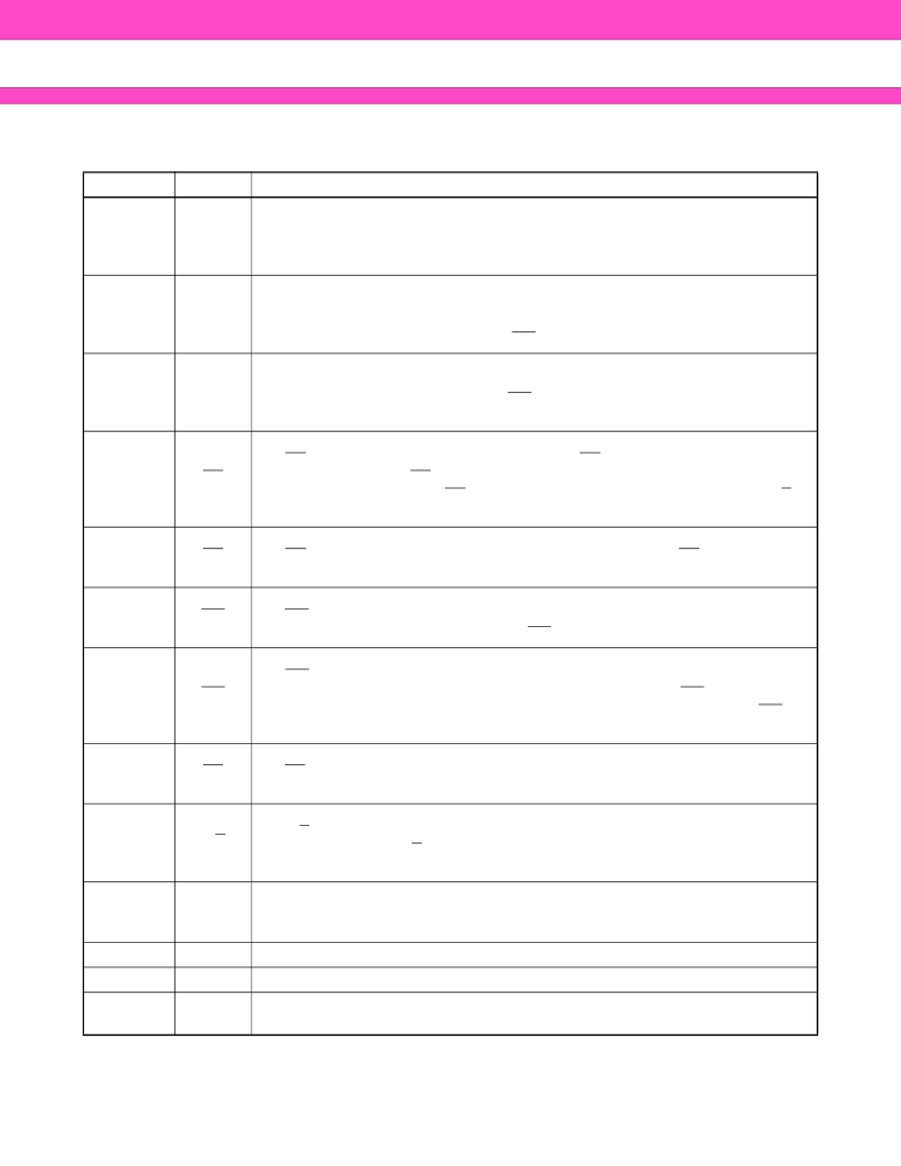
PIN DESCRIPTIONS
Pin Number Pin Name
Descriptions
18 to 21
24 to 27
I/O0 to
I/O7
Data Input/Output
The I/O ports are used for transferring command, address, and input/output data into
and out of the device. The I/O pins will be high impedance when the outputs are dis-
abled or the device is not selected.
2
CLE
Command Latch Enable
The CLE signal enables the acquisition of the made command into the internal com-
mand register. When CLE=“H”, command are latched into the command register from
the I/O port upon the rising edge of the WE signal.
3
ALE
Address Latch Enable
The ALE signal enables the acquisition of either address or data into the internal ad-
dress/data register. The rising edge of WE latch in addresses when ALE is high and
data when ALE is low.
43
CE
Chip Enable
The CE signal is used to select the device. When CE is high, the device enters a low
power standby mode. If CE transitions high during a read operation, the standby mode
will be entered. However, the CE signal is ignored if the device is in a busy state(R/B=L)
during a program or erase operation.
42
RE
Read Enable
The RE signal controls the serial data output. The falling edge of RE drives the data
onto the I/O bus and increments the column address counter by one.
4
WE
Write Enable
The WE signal controls writes from the I/O port. Data, address, and commands on the
I/O port are latched upon the rising of the WE pulse.
5
WP
Write Protect
The WP signal protects the device against accidental erasure or programming during
power up/down by disabling the internal high voltage generators. WP should be kept
low when the device powers up until V
CC
is above 2.5 V. During power down, WP
should be low when V
CC
falls below 2.5 V.
40
SE
Spare Area Enable
The SE input enables the spare area during sequential data input, page program, and
Read 1.
41
R/B
Ready Busy Output
The R/B output signal is used to indicate the operating status of the device. During pro-
gram, erase, or read, R/B is low and will return high upon the completion of the opera-
tion. The output buffer for this signal is an open drain.
23
V
CC
q
Output Buffer Power Supply
The V
CC
q input supplies the power to the I/O interface logic. This power line is electri-
cally isolated from V
CC
for the purpose of supporting 5V tolerant I/O.
44
V
CC
Power Supply
1,22
V
SS
Ground
6 to 17
28 to 39
N.C.
No Connection
相關PDF資料 |
PDF描述 |
|---|---|
| MBPC-200-5825 | NS Geode SBC with CPU, 4 COMs, Audio, VGA/LCD and Ethernet |
| MBR0520LTI | DB-LM3S102 Daughterboard |
| MBR1100 | SCHOTTKY BARRIER RECTIFIER 1.0 AMPERE 100 VOLTS |
| MBR1100RL | SCHOTTKY BARRIER RECTIFIER 1.0 AMPERE 100 VOLTS |
| MBR130LSFT1 | Surface Mount Schottky Power Rectifier Plastic SOD−123 Package |
相關代理商/技術參數 |
參數描述 |
|---|---|
| MBM31048901 | 制造商:LG Corporation 功能描述:Card |
| MBM31262801 | 制造商:LG Corporation 功能描述:Card,Technical |
| MBM31262802 | 制造商:LG Corporation 功能描述:Card,Technical |
| MBM31885001 | 制造商:LG Corporation 功能描述:Card,Information |
| MBM31885002 | 制造商:LG Corporation 功能描述:Card,Information |
發布緊急采購,3分鐘左右您將得到回復。