- 您現(xiàn)在的位置:買賣IC網(wǎng) > PDF目錄192295 > S25FL004D (Spansion Inc.) 4 Megabit CMOS 3.0 Volt Flash Memory with 50 Mhz SPI Bus Interface PDF資料下載
參數(shù)資料
| 型號: | S25FL004D |
| 廠商: | Spansion Inc. |
| 英文描述: | 4 Megabit CMOS 3.0 Volt Flash Memory with 50 Mhz SPI Bus Interface |
| 中文描述: | 4兆位的CMOS閃存3.0伏,50赫茲的SPI總線接口 |
| 文件頁數(shù): | 10/36頁 |
| 文件大小: | 724K |
| 代理商: | S25FL004D |
第1頁第2頁第3頁第4頁第5頁第6頁第7頁第8頁第9頁當(dāng)前第10頁第11頁第12頁第13頁第14頁第15頁第16頁第17頁第18頁第19頁第20頁第21頁第22頁第23頁第24頁第25頁第26頁第27頁第28頁第29頁第30頁第31頁第32頁第33頁第34頁第35頁第36頁
18
S25FL Family (Serial Peripheral Interface) S25FL004D
S25FL004D_00A0 June 28, 2004
Ad va n c e
In f o rm a t i o n
or by driving Write Protect (W#) Low after setting the Status Register Write
Disable (SRWD) bit.
The only way to exit the Hardware Protected Mode (HPM) once entered is to pull
Write Protect (W#) High.
If Write Protect (W#) is permanently tied High, the Hardware Protected Mode
(HPM) can never be activated, and only the Software Protected Mode (SPM),
using the Block Protect (BP2, BP1, BP0) bits of the Status Register, can be used.
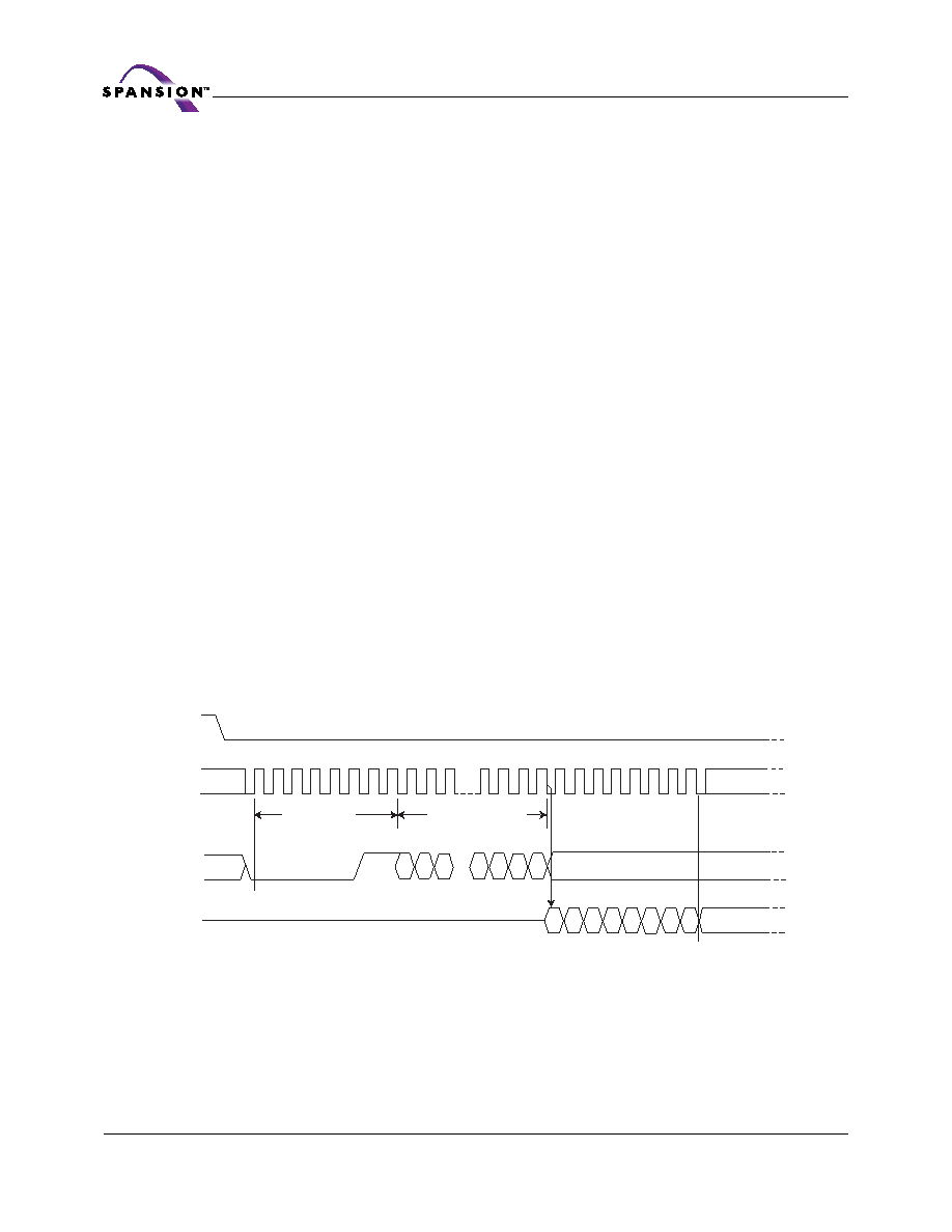
Read Data Bytes (READ)
The READ instruction reads the memory at the specified SCK frequency (fSCK)
with a maximum speed of 33 MHz.
The device is first selected by driving Chip Select (CS#) Low. The instruction code
for the Read Data Bytes (READ) instruction is followed by a 3-byte address (A23-
A0), each bit being latched-in during the rising edge of Serial Clock (SCK). Then
the memory contents, at that address, are shifted out on Serial Data Output
(SO), each bit being shifted out, at a frequency fSCK, during the falling edge of
Serial Clock (SCK).
The instruction sequence is shown in Figure 9. The first byte addressed can be at
any location. The address is automatically incremented to the next higher ad-
dress after each byte of data is shifted out. The whole memory can, therefore, be
read with a single Read Data Bytes (READ) instruction. When the highest address
is reached, the address counter rolls over to 00000h, allowing the read sequence
to be continued indefinitely.
The Read Data Bytes (READ) instruction is terminated by driving Chip Select
(CS#) High. Chip Select (CS#) can be driven High at any time during data output.
Any Read Data Bytes (READ) instruction, while a Program, Erase, or Write cycle
is in progress, is rejected without having any effect on the cycle that is in
progress.
Figure 9. Read Data Bytes (READ) Instruction Sequence
Read Data Bytes at Higher Speed (FAST_READ)
The FAST_READ instruction reads the memory at the specified SCK frequency
(fSCK) with a maximum speed of 50 MHz. The device is first selected by driving
Chip Select (CS#) Low. The instruction code for (FAST_READ) instruction is fol-
lowed by a 3-byte address (A23-A0) and a dummy byte, each bit being latched-
in during the rising edge of Serial Clock (SCK). Then the memory contents, at that
Instruction
24-Bit Address
High Impedance
MSB
Data Out 1
Data Out 2
0
31 32 33 34 35 36 37 38 39
30
23
28
10
9
8
7
6
5
4
3
2
1
7 6 5
23 22 21
4
3 2
1 0
3
2
1 0 7
SO
SI
SCK
CS#
相關(guān)PDF資料 |
PDF描述 |
|---|---|
| S25FL004D0LNAI011 | 4 Megabit CMOS 3.0 Volt Flash Memory with 50 Mhz SPI Bus Interface |
| S25FL004D0LNAI013 | 4 Megabit CMOS 3.0 Volt Flash Memory with 50 Mhz SPI Bus Interface |
| S25FL064A0LNAI00 | 64M X 1 FLASH 3V PROM, PDSO16 |
| S2684-254 | PHOTO DIODE |
| S2815S | 1-OUTPUT 10 W DC-DC REG PWR SUPPLY MODULE |
相關(guān)代理商/技術(shù)參數(shù) |
參數(shù)描述 |
|---|---|
| S25FL004D0FMFI | 制造商:Spansion 功能描述: |
| S25FL004D0LMAI011 | 制造商:SPANSION 制造商全稱:SPANSION 功能描述:4 Megabit CMOS 3.0 Volt Flash Memory with 50 Mhz SPI Bus Interface |
| S25FL004D0LMAI013 | 制造商:SPANSION 制造商全稱:SPANSION 功能描述:4 Megabit CMOS 3.0 Volt Flash Memory with 50 Mhz SPI Bus Interface |
| S25FL004D0LMFI011 | 制造商:SPANSION 制造商全稱:SPANSION 功能描述:4 Megabit CMOS 3.0 Volt Flash Memory with 50 Mhz SPI Bus Interface |
| S25FL004D0LMFI013 | 制造商:SPANSION 制造商全稱:SPANSION 功能描述:4 Megabit CMOS 3.0 Volt Flash Memory with 50 Mhz SPI Bus Interface |
發(fā)布緊急采購,3分鐘左右您將得到回復(fù)。