- 您現在的位置:買賣IC網 > PDF目錄192295 > S25FL004D (Spansion Inc.) 4 Megabit CMOS 3.0 Volt Flash Memory with 50 Mhz SPI Bus Interface PDF資料下載
參數資料
| 型號: | S25FL004D |
| 廠商: | Spansion Inc. |
| 英文描述: | 4 Megabit CMOS 3.0 Volt Flash Memory with 50 Mhz SPI Bus Interface |
| 中文描述: | 4兆位的CMOS閃存3.0伏,50赫茲的SPI總線接口 |
| 文件頁數: | 2/36頁 |
| 文件大小: | 724K |
| 代理商: | S25FL004D |
第1頁當前第2頁第3頁第4頁第5頁第6頁第7頁第8頁第9頁第10頁第11頁第12頁第13頁第14頁第15頁第16頁第17頁第18頁第19頁第20頁第21頁第22頁第23頁第24頁第25頁第26頁第27頁第28頁第29頁第30頁第31頁第32頁第33頁第34頁第35頁第36頁
10
S25FL Family (Serial Peripheral Interface) S25FL004D
S25FL004D_00A0 June 28, 2004
Ad va n c e
In f o rm a t i o n
Protection Modes
The SPI memory device boasts the following data protection mechanisms:
All instructions that modify data must be preceded by a Write Enable (WREN)
instruction to set the Write Enable Latch (WEL) bit. This bit is returned to its
reset state by the following events:
—Power-up
— Write Disable (WRDI) instruction completion
— Write Status Register (WRSR) instruction completion
— Page Program (PP) instruction completion
— Sector Erase (SE) instruction completion
— Bulk Erase (BE) instruction completion
The Block Protect (BP2, BP1, BP0) bits allow part of the memory to be con-
figured as read-only. This is the Software Protected Mode (SPM).
The Write Protect (W#) signal works in cooperation with the Status Register
Write Disable (SRWD) bit to enable write-protection. This is the Hardware
Protected Mode (HPM).
Program, Erase and Write Status Register instructions are checked to verify
that they consist of a number of clock pulses that is a multiple of eight, before
they are accepted for execution.
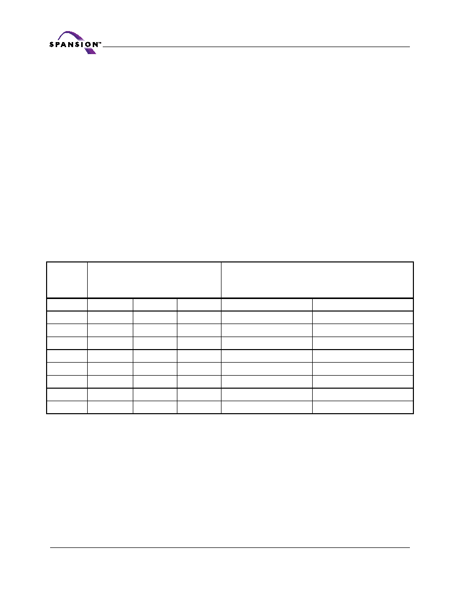
Table 1. Protected Area Sizes (S25FL004D).
Hold Condition Modes
The Hold (HOLD#) signal is used to pause any serial communications with the
device without resetting the clocking sequence. Hold (HOLD#) signal gates the
clock input to the device. However, taking this signal Low does not terminate any
Write Status Register, Program or Erase Cycle that is currently in progress.
To enter the Hold condition, the device must be selected, with Chip Select (CS#)
Low. The Hold condition starts on the falling edge of the Hold (HOLD#) signal,
provided that this coincides with Serial Clock (SCK) being Low (as shown in Figure
The Hold condition ends on the rising edge of the Hold (HOLD#) signal, provided
that this coincides with Serial Clock (SCK) being Low.
Protected
Memory
Area
(Top Level)
Status Register Content
Memory Content
BP2 Bit
BP1 Bit
BP0
Protected Area
Unprotected Area
0
none
00000–7FFFF
1/8
0
1
70000–7FFFF
00000–6FFFF
1/4
0
1
0
60000–7FFFF
00000–5FFFF
1/2
0
1
40000–7FFFF
00000–3FFFF
All
1
0
00000-7FFFF
none
All
1
0
1
00000-7FFFF
none
All
1
0
00000-7FFFF
none
All
1
00000-7FFFF
none
相關PDF資料 |
PDF描述 |
|---|---|
| S25FL004D0LNAI011 | 4 Megabit CMOS 3.0 Volt Flash Memory with 50 Mhz SPI Bus Interface |
| S25FL004D0LNAI013 | 4 Megabit CMOS 3.0 Volt Flash Memory with 50 Mhz SPI Bus Interface |
| S25FL064A0LNAI00 | 64M X 1 FLASH 3V PROM, PDSO16 |
| S2684-254 | PHOTO DIODE |
| S2815S | 1-OUTPUT 10 W DC-DC REG PWR SUPPLY MODULE |
相關代理商/技術參數 |
參數描述 |
|---|---|
| S25FL004D0FMFI | 制造商:Spansion 功能描述: |
| S25FL004D0LMAI011 | 制造商:SPANSION 制造商全稱:SPANSION 功能描述:4 Megabit CMOS 3.0 Volt Flash Memory with 50 Mhz SPI Bus Interface |
| S25FL004D0LMAI013 | 制造商:SPANSION 制造商全稱:SPANSION 功能描述:4 Megabit CMOS 3.0 Volt Flash Memory with 50 Mhz SPI Bus Interface |
| S25FL004D0LMFI011 | 制造商:SPANSION 制造商全稱:SPANSION 功能描述:4 Megabit CMOS 3.0 Volt Flash Memory with 50 Mhz SPI Bus Interface |
| S25FL004D0LMFI013 | 制造商:SPANSION 制造商全稱:SPANSION 功能描述:4 Megabit CMOS 3.0 Volt Flash Memory with 50 Mhz SPI Bus Interface |
發布緊急采購,3分鐘左右您將得到回復。