- 您現(xiàn)在的位置:買賣IC網(wǎng) > PDF目錄192295 > S29AL032D90TFI043 (SPANSION LLC) 32 Megabit CMOS 3.0 Volt-only Flash Memory PDF資料下載
參數(shù)資料
| 型號: | S29AL032D90TFI043 |
| 廠商: | SPANSION LLC |
| 元件分類: | PROM |
| 英文描述: | 32 Megabit CMOS 3.0 Volt-only Flash Memory |
| 中文描述: | 2M X 16 FLASH 3V PROM, 90 ns, PDSO48 |
| 封裝: | LEAD FREE, MO-142DD, TSOP-48 |
| 文件頁數(shù): | 36/67頁 |
| 文件大小: | 1708K |
| 代理商: | S29AL032D90TFI043 |
第1頁第2頁第3頁第4頁第5頁第6頁第7頁第8頁第9頁第10頁第11頁第12頁第13頁第14頁第15頁第16頁第17頁第18頁第19頁第20頁第21頁第22頁第23頁第24頁第25頁第26頁第27頁第28頁第29頁第30頁第31頁第32頁第33頁第34頁第35頁當(dāng)前第36頁第37頁第38頁第39頁第40頁第41頁第42頁第43頁第44頁第45頁第46頁第47頁第48頁第49頁第50頁第51頁第52頁第53頁第54頁第55頁第56頁第57頁第58頁第59頁第60頁第61頁第62頁第63頁第64頁第65頁第66頁第67頁
November 2, 2006 S29AL032D_00_A8
S29AL032D
39
Data
She e t
Legend
Notes
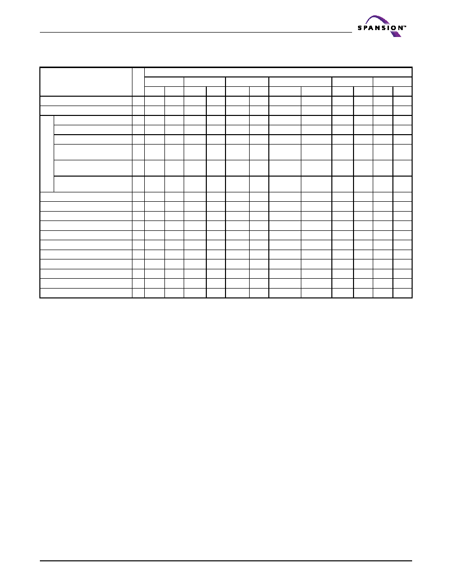
Table 11.3 S29AL032D Command Definitions, x16 Mode — Models 03, 04
Command Sequence
Cyc
le
s
Bus Cycles (Notes 2–5)
First
Second
Third
Fourth
Fifth
Sixth
Addr
Data
Addr
Data
Addr
Data
Addr
Data
Addr
Data
Addr
Data
Read (Note 6)
1RA
RD
Reset (Note 7)
1XXX
F0
A
u
toselect
Manufacturer ID
4
555
AA
2AA
55
555
90
X00
01
Device ID, Model 03
4
555
AA
2AA
55
555
90
X01
22F6
Device ID, Model 04
4
555
AA
2AA
55
555
90
X01
22F9
Secured Silicon Sector Factory
Protect, Model 03 (Note 9)
4
555
AA
2AA
55
555
90
X03
8D/0D
Secured Silicon Sector Factory
Protect, Model 04 (Note 9)
4
555
AA
2AA
55
555
90
X03
9D/1D
Sector Protect Verify
4
555
AA
2AA
55
555
90
(SA)X02
Enter Secured Silicon Sector Region
3
555
AA
2AA
55
555
88
Exit Secured Silicon Sector Region
4
555
AA
2AA
55
555
90
XXX
00
CFI Query (Note 11)
155
98
Program
4
555
AA
2AA
55
555
A0
PA
PD
Unlock Bypass
3
555
AA
2AA
55
555
20
Unlock Bypass Program (Note 12)
2
XXX
A0
PA
PD
Unlock Bypass Reset (Note 13)
2
XXX
90
XXX
00
Chip Erase
6
555
AA
2AA
55
555
80
555
AA
2AA
55
555
10
Sector Erase
6
555
AA
2AA
55
555
80
555
AA
2AA
55
SA
30
Erase Suspend (Note 14)
1
XXX
B0
Erase Resume (Note 15)
1XXX
30
X = Don’t care
RA = Address of the memory location to be read
RD = Data read from location RA during read operation
PA = Address of the memory location to be programmed. Addresses are latched
on the falling edge of the WE# or CE# pulse, whichever happens later.
PD = Data to be programmed at location PA. Data is latched on the rising edge
of WE# or CE# pulse, whichever happens first.
SA = Address of the sector to be erased or verified. Address bits A19–A12
uniquely select any sector.
1. See Table 7.1 on page 12 for description of bus operations.
2. All values are in hexadecimal.
3. Except for the read cycle and the fourth cycle of the autoselect command
sequence, all bus cycles are write cycles.
4. Data bits DQ15–DQ8 are don’t cares for unlock and command cycles.
5. Address bits A19–A11 are don’t cares for unlock and command cycles,
unless SA or PA required.
6. No unlock or command cycles required when reading array data.
7. The Reset command is required to return to reading array data when device
is in the autoselect mode, or if DQ5 goes high (while the device is providing
status data).
8. The fourth cycle of the autoselect command sequence is a read cycle.
9. For Model 03, the data is 8Dh for factory locked and 0Dh for not factory
locked. For Model 04, the data is 9Dh for factory locked and 1Dh for not
factory locked.
10. The data is 00h for an unprotected sector and 01h for a protected sector.
See “Autoselect Command Sequence”for more information.
11. Command is valid when device is ready to read array data or when device is
in autoselect mode.
12. The Unlock Bypass command is required prior to the Unlock Bypass
Program command.
13. The Unlock Bypass Reset command is required to return to reading array
data when the device is in the unlock bypass mode. F0 is also acceptable.
14. The system may read and program in non-erasing sectors, or enter the
autoselect mode, when in the Erase Suspend mode. The Erase Suspend
command is valid only during a sector erase operation.
15. The Erase Resume command is valid only during the Erase Suspend mode.
相關(guān)PDF資料 |
PDF描述 |
|---|---|
| S29CD016G0JDEI004 | 512K X 32 FLASH 2.7V PROM, 67 ns, UUC76 |
| S29CD016G0JDEI007 | 512K X 32 FLASH 2.7V PROM, 67 ns, UUC76 |
| S29CD032J1JFAI122 | 1M X 32 FLASH 2.7V PROM, 54 ns, PBGA80 |
| S29CD032J1MFAN120 | 1M X 32 FLASH 2.7V PROM, 54 ns, PBGA80 |
| S29CD032J1MQFN133 | 1M X 32 FLASH 2.7V PROM, 54 ns, PQFP80 |
相關(guān)代理商/技術(shù)參數(shù) |
參數(shù)描述 |
|---|---|
| S29AS008J70BFI030 | 功能描述:閃存 8Mb 3V 70ns Parallel NOR 閃存 RoHS:否 制造商:ON Semiconductor 數(shù)據(jù)總線寬度:1 bit 存儲類型:Flash 存儲容量:2 MB 結(jié)構(gòu):256 K x 8 定時類型: 接口類型:SPI 訪問時間: 電源電壓-最大:3.6 V 電源電壓-最小:2.3 V 最大工作電流:15 mA 工作溫度:- 40 C to + 85 C 安裝風(fēng)格:SMD/SMT 封裝 / 箱體: 封裝:Reel |
| S29AS008J70BFI032 | 制造商:Spansion 功能描述:8 MEG CMOS 1.8 VOLT-ONLY BOOT SECTOR FLASH MEMORY - Trays |
| S29AS008J70BFI042 | 制造商:Spansion 功能描述:8 MEG CMOS 1.8 VOLT-ONLY BOOT SECTOR FLASH MEMORY - Trays |
| S29AS008J70TFI030 | 功能描述:閃存 8Mb 1.8V 70ns Parallel NOR 閃存 RoHS:否 制造商:ON Semiconductor 數(shù)據(jù)總線寬度:1 bit 存儲類型:Flash 存儲容量:2 MB 結(jié)構(gòu):256 K x 8 定時類型: 接口類型:SPI 訪問時間: 電源電壓-最大:3.6 V 電源電壓-最小:2.3 V 最大工作電流:15 mA 工作溫度:- 40 C to + 85 C 安裝風(fēng)格:SMD/SMT 封裝 / 箱體: 封裝:Reel |
| S29AS008J70TFI040 | 功能描述:閃存 8Mb 1.8V 70ns Parallel NOR 閃存 RoHS:否 制造商:ON Semiconductor 數(shù)據(jù)總線寬度:1 bit 存儲類型:Flash 存儲容量:2 MB 結(jié)構(gòu):256 K x 8 定時類型: 接口類型:SPI 訪問時間: 電源電壓-最大:3.6 V 電源電壓-最小:2.3 V 最大工作電流:15 mA 工作溫度:- 40 C to + 85 C 安裝風(fēng)格:SMD/SMT 封裝 / 箱體: 封裝:Reel |
發(fā)布緊急采購,3分鐘左右您將得到回復(fù)。