- 您現在的位置:買賣IC網 > PDF目錄24691 > 05F7355 IC-SM-SWITCH ARRAY PDF資料下載
參數資料
| 型號: | 05F7355 |
| 英文描述: | IC-SM-SWITCH ARRAY |
| 中文描述: | 集成電路釤開關陣列 |
| 文件頁數: | 1/4頁 |
| 文件大小: | 72K |
| 代理商: | 05F7355 |
REV. C
Information furnished by Analog Devices is believed to be accurate and
reliable. However, no responsibility is assumed by Analog Devices for its
use, nor for any infringements of patents or other rights of third parties
which may result from its use. No license is granted by implication or
otherwise under any patent or patent rights of Analog Devices.
a
AD75019
One Technology Way, P.O. Box 9106, Norwood, MA 02062-9106, U.S.A.
Tel: 781/329-4700
World Wide Web Site: http://www.analog.com
Fax: 781/326-8703
Analog Devices, Inc., 1999
16
16 Crosspoint
Switch Array
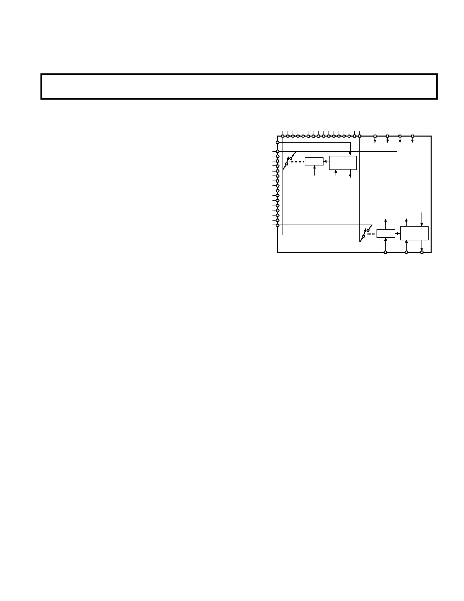
FUNCTIONAL BLOCK DIAGRAM
SHIFT
REGISTER
CELL #256
LATCH
SERIAL DATA IN
ANALOG
SWITCH
BUSED CLOCK
LINES
SERIAL
DATA
TO NEXT
STAGES
+12V –12V
+5V
DGND
AD75019
16
16 ARRAY OF SWITCHES,
LATCHES, AND SHIFT REGISTER
CELLS (ONLY TWO LOCATIONS
ARE SHOWN FOR CLARITY)
SHIFT
REGISTER
CELL #1
LATCH
ANALOG
SWITCH
PARALLEL
CLOCK
SERIAL
CLOCK
SERIAL
DATA
FROM
PRIOR
STAGES
BUSED CLOCK
LINES
VDD
VSS
VCC DGND
X0
X15
ANALOG
INPUTS/OUTPUTS
Y0
Y15
ANALOG
OUTPUTS/
INPUTS
PCLK
SCLK
SOUT
FEATURES
256 Switches in a 16
16 Array
Wide Signal Range: to Supply Rails of 24 V or
12 V
Low On-Resistance: 200
Typ
TTL/CMOS/Microprocessor-Compatible Control Lines
Serial Input Simplifies Interface
Serial Output Allows Cascading for More Channels
Low Power Consumption: 2 mW Quiescent
Compact 44-Lead PLCC
PRODUCT DESCRIPTION
The AD75019 contains 256 analog switches in a 16
× 16 array.
Any of the X or Y pins may serve as an input or output. Any or
all of the X terminals may be programmed to connect to any or
all of the Y terminals. The switches can accommodate signals
with amplitudes up to the supply rails and have a typical on-
resistance of 150
.
Data is loaded serially via the SIN input and clocked into an on-
board 256-bit shift register via SCLK. When all the switch set-
tings have been programmed, data is transferred into a set of
256 latches via PCLK. The serial shift register is dynamic, so
there is a minimum clock rate of 20 kHz. The maximum clock
rate of 5 MHz allows loading times as short as 52
s. The switch
control latches are static and will hold their data as long as power
is applied.
To extend the number of switches in the array, you may cascade
multiple AD75019s. The SOUT output is the end of the shift
register, and may be connected to the SIN input of the next
AD75019.
The AD75019 is fabricated in Analog Devices’ BiMOS II
process. This epitaxial BiCMOS process features CMOS
devices for low distortion switches and bipolar devices for
ESD protection.
相關PDF資料 |
PDF描述 |
|---|---|
| 934050540135 | 2.6 A, 55 V, 0.15 ohm, N-CHANNEL, Si, POWER, MOSFET |
| 934050550135 | 3.5 A, 55 V, 0.08 ohm, N-CHANNEL, Si, POWER, MOSFET |
| 934050610114 | L BAND, Si, NPN, RF POWER TRANSISTOR |
| 934050960135 | 100 mA, 40 V, PNP, Si, SMALL SIGNAL TRANSISTOR |
| 934050950115 | 100 mA, 40 V, PNP, Si, SMALL SIGNAL TRANSISTOR |
相關代理商/技術參數 |
參數描述 |
|---|---|
| 05FD101J03 | 制造商: 功能描述: 制造商:undefined 功能描述: |
| 05FD111J03 | 制造商: 功能描述: 制造商:undefined 功能描述: |
| 05FD161J03 | 制造商: 功能描述: 制造商:undefined 功能描述: |
| 05FD241J03 | 制造商: 功能描述: 制造商:undefined 功能描述: |
| 05FD271J03 | 制造商: 功能描述: 制造商:undefined 功能描述: |
發布緊急采購,3分鐘左右您將得到回復。