- 您現在的位置:買賣IC網 > Datasheet目錄38 > 1B22AN (Analog Devices Inc)IC VOLTAGE CONVERTER PROG DIP Datasheet資料下載
參數資料
| 型號: | 1B22AN |
| 廠商: | Analog Devices Inc |
| 文件頁數: | 2/4頁 |
| 文件大小: | 224K |
| 描述: | IC VOLTAGE CONVERTER PROG DIP |
| 產品變化通告: | Product Change Notice 06/Jul/2009 |
| 標準包裝: | 1 |
| 類型: | 電壓和電流控制器 |
| 全量程: | ±50ppm/°C |
| 線性: | ±0.02% |
| 安裝類型: | 通孔 |
| 封裝/外殼: | 38-DIP(0.800",20.32mm),12 引線 |
| 供應商設備封裝: | 12-DIP |
| 包裝: | 散裝 |
REV. B
2
1B22SPECIFICATIONS
(typical @ +25C and V
S
= 15 V, V
LOOP
= +24 V, unless otherwise noted)
Model
1B22AN
INPUT SPECIFICATIONS
Factory Calibrated, User Selectable
0 V to +5 V, 0 V to +10 V
Input Impedance
0 V to +10 V Input Range
50 k&
0 V to +5 V Input Range
25 k&
OUTPUT SPECIFICATIONS
Current Output Range, User Selectable
4 to 20 mA, 0 to 20 mA
Load Compliance Range, V
LOOP
= +15 V
8 V min
Load Compliance Range, V
LOOP
= +28 V
20 V min
Maximum Output Current @ Input Overload 30 mA
Output Noise, 100 Hz Bandwidth
300 nA p-p
NONLINEARITY (% of Span)
?.02% (?.05% max)
ISOLATION
CMV, Input to Output Continuous
1500 V rms max
CMR, @ 60 Hz
90 dB min
Normal-Mode Output Protection
240 V rms Continuous
CMV Transient Protection
IEEE-STD 472 (SWC)
ACCURACY
Warm-Up Time to Rated Performance
5 min
Total Output Error @ +25癈
Offset (V
IN
= 0 V)
?0 礎
Span (V
IN
= +10 V)
?.7% Full Scale
vs. Temperature (25癈 to +85癈)
Offset
?00 nA/癈
Span
?0 ppm/癈
DYNAMIC RESPONSE
Settling Time to 0.1% of FS for 10 V Step
9 ms
Small Signal Bandwidth
400 Hz
POWER SUPPLY
Bipolar Input Supplies
Operating Voltage
?5 V ?5%
Quiescent Current
?.5 mA
Power Supply Rejection
?.01%/V
Loop Supply
Operating Voltage
+14 V to +30 V
Operating Current, at Full-Scale Output
25 mA
Loop Supply Rejection
?.005%/V
ENVIRONMENTAL
Temperature Range
Rated Performance
25癈 to +85癈
Operating
40癈 to +85癈
Storage
40癈 to +85癈
Relative Humidity, Noncondensing
0 to 95% @ 60癈
CASE SIZE
1.0" ?2.1" ?0.35"
Specifications subject to change without notice.
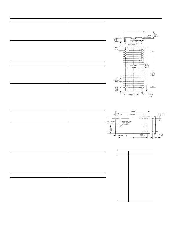
OUTLINE DIMENSIONS
Dimensions shown in inches and (mm).
AC1225 MATING SOCKET
PIN DESIGNATIONS
Pin
Function
11
OUT HI
16
IN2
17
IN1
18
S. NODE
19
4 mA OFFSET
20
+15 V
21
ANA COM
22
15 V
23
SYNC
24
V
LOOP
25
POWER COM
38
OUT LO
相關PDF資料 |
PDF描述 |
|---|---|
| AD536AKQ | IC TRUE RMS/DC CONV 14CDIP |
| AD537SD | IC V/F CONV 14-CDIP |
| AD636JD | IC TRUE RMS/DC CONV MONO 14-CDIP |
| AD650SD | IC V-F/F-V CONV 1MHZ 14-CDIP |
| AD652SQ | IC V-F CONV SYNCH MONO 5V 16CDIP |
相關代理商/技術參數 |
參數描述 |
|---|---|
| 1B22AN | 制造商:Analog Devices 功能描述:SEMICONDUCTORSLINEAR 制造商:Analog Devices 功能描述:IC, VOLTAGE-TO-CURRENT CONVERTER, 12-DIP |
| 1B-23A-B | 制造商:FCI 功能描述: |
| 1B243 | 制造商:Ferraz Shawmut 功能描述: |
| 1B245 | 制造商:Ferraz Shawmut 功能描述: |
| 1B-24A | 制造商:FCI 功能描述:CONN CONT M/M 1 POS/1 POS ST - Tape and Reel |
發布緊急采購,3分鐘左右您將得到回復。