- 您現在的位置:買賣IC網 > PDF目錄370043 > 2N5547 (Vishay Intertechnology,Inc.) Monolithic Dual N-Channel JFET(最小柵源擊穿電壓-50V,最大柵極工作電流-50pA的雙N溝道結型場效應管) PDF資料下載
參數資料
| 型號: | 2N5547 |
| 廠商: | Vishay Intertechnology,Inc. |
| 英文描述: | Monolithic Dual N-Channel JFET(最小柵源擊穿電壓-50V,最大柵極工作電流-50pA的雙N溝道結型場效應管) |
| 中文描述: | 單片雙N溝道場效應(最小柵源擊穿電壓- 50V的最大柵極工作電流,50pA的的雙?溝道結型場效應管) |
| 文件頁數: | 1/5頁 |
| 文件大小: | 75K |
| 代理商: | 2N5547 |
2N5545/46/47/JANTX/JANTXV
Siliconix
P-37514—Rev. B, 25-Jul-94
1
Monolithic N-Channel JFET Duals
Product Summary
Part Number
V
GS(off)
(V)
V
(BR)GSS
Min (V)
g
fs
Min (mS)
I
G
Max (pA)
V
GS1
– V
GS2
Max (mV)
2N5545
–0.5 to –4.5
–50
1.5
–50
5
2N5546
–0.5 to –4.5
–50
1.5
–50
10
2N5547
–0.5 to –4.5
–50
1.5
–50
15
Features
Monolithic Design
High Slew Rate
Low Offset/Drift Voltage
Low Gate Leakage: 3 pA
Low Noise
High CMRR: 100 dB
Benefits
Tight Differential Match vs. Current
Improved Op Amp Speed, Settling Time Accuracy
Minimum Input Error/Trimming Requirement
Insignificant Signal Loss/Error Voltage
High System Sensitivity
Minimum Error with Large Input Signal
Applications
Wideband Differential Amps
High-Speed,
Temp-Compensated,
Single-Ended Input Amps
High-Speed Comparators
Impedance Converters
Description
The 2N5545/5546/5547JANTX/JANTXV are monolithic
dual n-channel JFETs designed to provide high input
impedance (I
G
< 50 pA) for general-purpose differential
amplifiers. The 2N5545 features minimum system error
and calibration (5-mV offset maximum).
The TO-71 package is available with full military
processing (see Military Information).
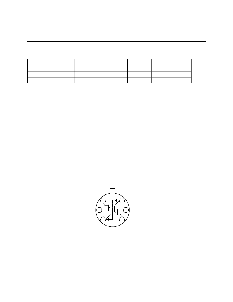
TO-71
Top View
G
1
S
1
D
1
G
2
D
2
S
2
1
2
3
6
5
4
Absolute Maximum Ratings
Gate-Drain, Gate-Source Voltage
Gate Current
. . . . . . . . . . . . . . . . . . . . . . . . . . . . . . . . . . . . . . . .
Lead Temperature (
1
/
16
” from case for 10 sec.)
Storage Temperature
. . . . . . . . . . . . . . . . . . . . . . . . . . .
Operating Junction Temperature
–50 V
30 mA
300 C
. . . . . . . . . . . . . . . . . . . . . . . .
. . . . . . . . . . . . .
–65 to 200 C
–55 to 150 C
. . . . . . . . . . . . . . . . . .
Power Dissipation :
Per Side
a
Total
b
250 mW
500 mW
. . . . . . . . . . . . . . . . .
. . . . . . . . . . . . . . . . . . . .
Notes
a.
b.
Derate 2 mW/ C above 25 C
Derate 4 mW/ C above 25 C
Updates to this data sheet may be obtained via facsimile by calling Siliconix FaxBack, 1-408-970-5600. Please request FaxBack document #70253.
相關PDF資料 |
PDF描述 |
|---|---|
| 2N5564 | Matched N-Channel JFET Pairs(最小柵源擊穿電壓-40V,柵極工作電流-3pA的N溝道結型場效應管) |
| 2N5565 | Matched N-Channel JFET Pairs(最小柵源擊穿電壓-40V,柵極工作電流-3pA的N溝道結型場效應管) |
| 2N5566 | Matched N-Channel JFET Pairs(最小柵源擊穿電壓-40V,柵極工作電流-3pA的N溝道結型場效應管) |
| 2N5633 | SILICON POWER TRANSISTOR |
| 2N5634 | SILICON POWER TRANSISTOR |
相關代理商/技術參數 |
參數描述 |
|---|---|
| 2N5547JANTX | 制造商:VISHAY 制造商全稱:Vishay Siliconix 功能描述:Monolithic N-Channel JFET Duals |
| 2N5547JANTXV | 制造商:VISHAY 制造商全稱:Vishay Siliconix 功能描述:Monolithic N-Channel JFET Duals |
| 2N5547JTX01 | 制造商:Vishay Siliconix 功能描述:19500/430 JANTX2N5547 |
| 2N5547JTX02 | 制造商:Vishay Siliconix 功能描述:TRANS JFET N-CH 6PIN TO-71 - Bulk |
| 2N5547JTXL01 | 制造商:Vishay Siliconix 功能描述:19500/430 JANTX2N5547 W/SOLDER DIP |
發布緊急采購,3分鐘左右您將得到回復。