- 您現在的位置:買賣IC網 > PDF目錄369113 > 2SC4073 (SANKEN ELECTRIC CO LTD) Isolated Flyback Switching Regulator with 9V Output PDF資料下載
參數資料
| 型號: | 2SC4073 |
| 廠商: | SANKEN ELECTRIC CO LTD |
| 元件分類: | 功率晶體管 |
| 英文描述: | Isolated Flyback Switching Regulator with 9V Output |
| 中文描述: | 5 A, 400 V, NPN, Si, POWER TRANSISTOR, TO-220AB |
| 封裝: | TO-220F, 3 PIN |
| 文件頁數: | 1/1頁 |
| 文件大小: | 25K |
| 代理商: | 2SC4073 |
87
Silicon NPN Triple Diffused Planar Transistor
(High Voltage and High Speed Switchihg Transistor)
Application :
Switching Regulator and General Purpose
Symbol
V
CBO
V
CEO
V
EBO
I
C
I
B
P
C
Tj
T
stg
2SC4073
500
400
10
5(
Pulse
10)
2
30(Tc=25°C)
150
–55 to +150
Unit
V
V
V
A
A
W
°C
°C
I
Absolute maximum ratings
I
Electrical Characteristics
Symbol
I
CBO
I
EBO
V
(BR)CEO
h
FE
V
CE
(sat)
V
BE
(sat)
f
T
C
OB
2SC4073
100
max
100
max
400
min
10to30
0.5
max
1.3
max
10
typ
30
typ
Unit
μ
A
μ
A
V
V
V
MHz
pF
Conditions
V
CB
=500V
V
EB
=10V
I
C
=25mA
V
CE
=4V, I
C
=2A
I
C
=2A, I
B
=0.4A
I
C
=2A, I
B
=0.4A
V
CE
=12V, I
E
=–0.3A
V
CB
=10V, f=1MHz
2S C4073
(Ta=25°C)
(Ta=25°C)
I
C
–V
CE
Characteristics
(Typical)
h
FE
–I
C
Characteristics
(Typical)
t
on
t
stg
t
f
–I
C
Characteristics
(Typical)
θ
j-a
–t
Characteristics
I
C
–V
BE
Temperature
Characteristics
(Typical)
V
CE
(sat),V
BE
(sat)–I
C
Temperature Characteristics
(Typical)
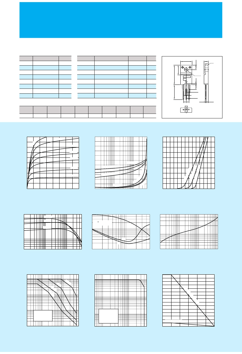
C
C
(
B
B
(
Pc–Ta Derating
Reverse Bias Safe Operating Area
Safe Operating Area
(Single Pulse)
0
0
1
2
3
4
5
2
1
3
4
Collector-Emitter Voltage V
CE
(V)
C
C
(
600mA
400mA
300mA
200mA
I
B
=800mA
100mA
50mA
0.01
0.1
0.05
1
5
0.5
0
2
1
(I
C
/I
B
=5)
Collector Current I
C
(A)
V
BE
(sat)
125C (Case Temp)
25C (Case Temp)
–55C (Case Temp)
2
–55C
V
CE
(sat)
1
2
5
C
C
a
s
e
e
m
p
)
0.1
1
0.5
5
0.1
0.5
5
1
S
t
o
t
s
t
f
(
μ
s
Collector Current I
C
(A)
t
stg
t
on
t
f
V
CC
200V
I
C
:I
B1
:–I
B2
=10:1:2
0.3
1
5
0.5
1
10
100
1000
Time t(ms)
T
θ
j
(
30
20
10
2
00
25
50
75
100
125
150
Ambient Temperature Ta(C)
M
C
(
WthIninteheasnk
Without Heatsink
10
50
5
500
100
1
0.5
0.1
0.05
0.01
10
20
5
Collector-Emitter Voltage V
CE
(V)
C
C
(
Without Heatsink
Natural Cooling
L=3mH
I
B2
=–0.5A
Duty:less than1%
10
50
5
2
100
500
0.05
0.01
1
0.5
0.1
10
20
5
Collector-Emitter Voltage V
CE
(V)
C
C
(
Without Heatsink
Natural Cooling
DC
10ms
100
μ
s
1ms
0.01
0.1
0.05
1
5
0.5
5
10
50
Collector Current I
C
(A)
D
F
(V
CE
=4V)
125C
25C
–55C
0
2
1
4
3
5
0
1.4
1.2
0.4
0.6
0.8
1.0
0.2
Base-Emittor Voltage V
BE
(V)
C
C
(
(V
CE
=4V)
15CCsTm)
–Cem
I
Typical Switching Characteristics (Common Emitter)
V
CC
(V)
200
R
L
(
)
100
I
C
(A)
2
V
(V)
–5
I
B2
(A)
–0.4
t
on
(
μ
s)
1
max
t
stg
(
μ
s)
3
max
t
f
(
μ
s)
0.5
max
I
(A)
0.2
V
(V)
10
External Dimensions
FM20(TO220F)
3.3
±0.2
10.1
±0.2
4
±
1
±
1
8
±
0
±
3
±
2.54
2.54
1.35
±0.15
0.85
+0.2
-0.1
1.35
±0.15
2.2
±0.2
4.2
±0.2
2.8
c0.5
2.4
±0.2
0.45
+0.2
-0.1
B
E
C
a
b
Weight : Approx 2.0g
a. Type No.
b. Lot No.
相關PDF資料 |
PDF描述 |
|---|---|
| 2SC4081 | 2SC4097 / 2SC1741S |
| 2SC1740S | FILTER PLATE |
| 2SC5658 | 2SC4097 / 2SC1741S |
| 2SC4617Q | TRANSISTOR | BJT | NPN | 50V V(BR)CEO | 150MA I(C) | SOT-323 |
| 2SC4617R | SC70/µDFN, Single/Dual Low-Voltage, Low-Power µP Reset Circuits |
相關代理商/技術參數 |
參數描述 |
|---|---|
| 2SC4075 | 制造商:ISC 制造商全稱:Inchange Semiconductor Company Limited 功能描述:Silicon NPN Power Transistors |
| 2SC4075C | 制造商:未知廠家 制造商全稱:未知廠家 功能描述:TRANSISTOR | BJT | NPN | 300V V(BR)CEO | 200MA I(C) | TO-220 |
| 2SC4075D | 制造商:未知廠家 制造商全稱:未知廠家 功能描述:TRANSISTOR | BJT | NPN | 300V V(BR)CEO | 200MA I(C) | TO-220 |
| 2SC4075E | 制造商:未知廠家 制造商全稱:未知廠家 功能描述:TRANSISTOR | BJT | NPN | 300V V(BR)CEO | 200MA I(C) | TO-220 |
| 2SC4077 | 制造商:Distributed By MCM 功能描述:SUB ONLY TRANSISTOR TO-9230V .1A .3W ECB |
發布緊急采購,3分鐘左右您將得到回復。