- 您現在的位置:買賣IC網 > PDF目錄49996 > 2SK198R (PANASONIC CORP) 20 mA, 30 V, N-CHANNEL, Si, SMALL SIGNAL, JFET, TO-236 PDF資料下載
參數資料
| 型號: | 2SK198R |
| 廠商: | PANASONIC CORP |
| 元件分類: | 小信號晶體管 |
| 英文描述: | 20 mA, 30 V, N-CHANNEL, Si, SMALL SIGNAL, JFET, TO-236 |
| 封裝: | ROHS COMPLIANT, MINI3-G1, SC-59, 3 PIN |
| 文件頁數: | 1/4頁 |
| 文件大小: | 210K |
| 代理商: | 2SK198R |
Silicon Junction FETs (Small Signal)
1
Publication date: May 200
8
SJF00006DED
This product complies with the RoHS Directive (EU 2002/95/EC).
2SK0198 (2SK198)
Silicon N-channel junction FET
For low-frequency amplification
■ Features
High mutual conductance g
m
Low-noise characteristics
Mini type package, allowing downsizing of the sets and automatic
insertion through the tape/magazine packing
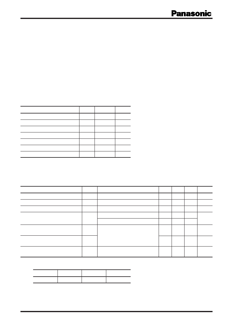
■ Absolute Maximum Ratings T
a
= 25°C
Parameter
Symbol
Rating
Unit
Drain-sourse voltage
VDS
30
V
Drain-gate voltage (Source open)
VDGO
30
V
Drain current
ID
20
mA
Gate current
IG
10
mA
Power dissipation
PD
150
mW
Channel temperature
Tch
150
°C
Storage temperature
Tstg
55 to +150
°C
Parameter
Symbol
Conditions
Min
Typ
Max
Unit
Drain-source current *
IDSS
VDS
= 10 V, V
GS
= 0
0.5
12
mA
Gate-source cutoff current
IGSS
VGS = 30 V, VDS = 0
100
nA
Gate-source cutoff voltage
VGSC
VDS = 10 V, ID = 10 A
0.1
1.5
V
Forward transfer admittance
Y
fs
VDS
= 10 V, I
D
= 0.5 mA, f = 1 kHz
4
mS
VDS = 10 V, VGS = 0, f = 1 kHz
4
Short-circuit forward transfer capacitance
Ciss
VDS = 10 V, VGS = 0, f = 1 MHz
14
pF
(Common source)
Reverse transfer capacitance
Crss
3.5
pF
(Common source)
Noise voltage
NV
VDS = 30 V, ID = 1 mA, GV = 80 dB
60
mV
Rg
= 100 k, Function = FLAT
■ Electrical Characteristics T
a
= 25°C ± 3°C
Note) 1. Measuring methods are based on JAPANESE INDUSTRIAL STANDARD JIS C 7030 measuring methods for transistors.
2. *: Rank classification
Rank
P
Q
R
IDSS (mA)
0.5 to 3.0
2.0 to 6.0
4.0 to 12.0
Note) The part number in the parenthesis shows conventional part number.
■ Package
Code
Mini3-G1
Pin Name
1: Source
2: Drain
3: Gate
■ Marking Symbol: 1O
Ma
int
en
an
ce
/
Dis
co
nti
nu
ed
Maintenance/Discontinued
includes
following
four
Product
lifecy
cle
stage.
planed
maintenance
type
maintenance
type
planed
discontinued
typed
discontinued
type
Please
visit
following
URL
about
latest
information.
http://panasonic.net/sc/en
相關PDF資料 |
PDF描述 |
|---|---|
| 2SK0198Q | 20 mA, 30 V, N-CHANNEL, Si, SMALL SIGNAL, JFET, TO-236 |
| 2SK1991 | 4.5 A, 100 V, 1.5 ohm, N-CHANNEL, Si, POWER, MOSFET |
| 2SK1990 | 4.5 A, 450 V, 1.4 ohm, N-CHANNEL, Si, POWER, MOSFET |
| 2SK1999 | RF POWER, FET |
| 2SK2008 | 20 A, 250 V, 0.15 ohm, N-CHANNEL, Si, POWER, MOSFET |
相關代理商/技術參數 |
參數描述 |
|---|---|
| 2SK19-GR | 制造商:Panasonic Industrial Company 功能描述:TRANSISTOR |
| 2SK19-Y | 制造商:Panasonic Industrial Company 功能描述:TRANSISTOR 2SK192A-Y |
| 2SK2000 | 制造商:FUJI 制造商全稱:Fuji Electric 功能描述:Power MOSFET |
| 2SK2000-R | 制造商:FUJI 制造商全稱:Fuji Electric 功能描述:Power MOSFET |
| 2SK2001-01M | 制造商:未知廠家 制造商全稱:未知廠家 功能描述:TRANSISTOR | MOSFET | N-CHANNEL | 350V V(BR)DSS | 15A I(D) | TO-220 |
發布緊急采購,3分鐘左右您將得到回復。