- 您現在的位置:買賣IC網 > PDF目錄56687 > 4N32-X010 (VISHAY SEMICONDUCTORS) 1 CHANNEL DARLINGTON OUTPUT OPTOCOUPLER PDF資料下載
參數資料
| 型號: | 4N32-X010 |
| 廠商: | VISHAY SEMICONDUCTORS |
| 元件分類: | 光電耦合器 |
| 英文描述: | 1 CHANNEL DARLINGTON OUTPUT OPTOCOUPLER |
| 封裝: | ROHS COMPLIANT, PLASTIC, DIP-6 |
| 文件頁數: | 2/6頁 |
| 文件大小: | 112K |
| 代理商: | 4N32-X010 |
www.vishay.com
For technical questions, contact: optocoupleranswers@vishay.com
Document Number: 81865
2
Rev. 1.1, 26-Oct-09
4N32, 4N33
Vishay Semiconductors
Optocoupler, Photodarlington
Output, High Gain, with Base
Connection
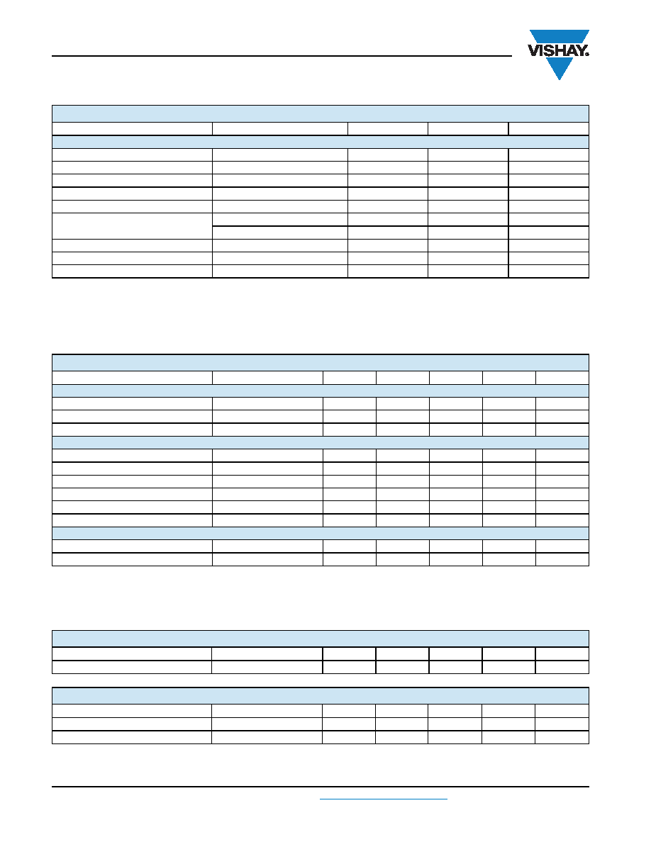
Notes
(1) Tamb = 25 °C, unless otherwise specified.
Stresses in excess of the absolute maximum ratings can cause permanent damage to the device. Functional operation of the device is not
implied at these or any other conditions in excess of those given in the operational sections of this document. Exposure to absolute
maximum ratings for extended periods of the time can adversely affect reliability.
(2) Refer to reflow profile for soldering conditions for surface mounted devices (SMD). Refer to wave profile for soldering conditions for through
hole devices (DIP).
Notes
(1) Tamb = 25 °C, unless otherwise specified.
Minimum and maximum values are testing requirements. Typical values are characteristics of the device and are the result of engineering
evaluation. Typical values are for information only and are not part of the testing requirements.
(2) Indicates JEDEC registered values.
COUPLER
Total dissipation
Ptot
250
mW
Derate linearly
3.3
mW/°C
Isolation test voltage (between emitter
1 s
VISO
5300
VRMS
Leakage path
7
mm min.
Air path
7
mm min.
Isolation resistance
VIO = 500 V, Tamb = 25 °C
RIO
≥ 1012
Ω
VIO = 500 V, Tamb = 100 °C
RIO
≥ 1011
Ω
Storage temperature
Tstg
- 55 to + 150
°C
Operating temperature
Tamb
- 55 to + 100
°C
Lead soldering time (2)
at 260 °C
10
s
ELECTRICAL CHARACTERISTICS (1)
PARAMETER
TEST CONDITION
SYMBOL
MIN.
TYP.
MAX.
UNIT
INPUT
Forward voltage
IF = 50 mA
VF
1.25
1.5
V
Reverse current
VR = 3 V
IR
0.1
100
μA
Capacitance
VR = 0 V
CO
25
pF
OUTPUT
Collector emitter breakdown voltage (2)
IC = 100 μA, IF = 0
BVCEO
30
V
Collector base breakdown voltage (2)
IC = 100 μA, IF = 0
BVCBO
50
V
Emitter base breakdown voltage (2)
IC = 100 μA, IF = 0
BVEBO
8V
Emitter collector breakdown voltage (2)
IC = 100 μA, IF = 0
BVECO
510
V
Collector emitter leakage current
VCE = 10 V, IF = 0
ICEO
1
100
nA
IC = 0.5 mA, VCE = 5 V
hFE
13
COUPLER
Collector emitter saturation voltage
VCEsat
1V
Coupling capacitance
1.5
pF
CURRENT TRANSFER RATIO
PARAMETER
TEST CONDITION
SYMBOL
MIN.
TYP.
MAX.
UNIT
Current transfer ratio
VCE = 10 V, IF = 10 mA
CTR
500
%
SWITCHING CHARACTERISTICS
PARAMETER
TEST CONDITION
SYMBOL
MIN.
TYP.
MAX.
UNIT
Turn-on time
VCC = 10 V, IC = 50 mA
ton
5μs
Turn-off time
IF = 200 mA, RL = 180 Ω
toff
100
μs
ABSOLUTE MAXIMUM RATINGS (1)
PARAMETER
TEST CONDITION
SYMBOL
VALUE
UNIT
相關PDF資料 |
PDF描述 |
|---|---|
| 4N33-X000 | 1 CHANNEL DARLINGTON OUTPUT OPTOCOUPLER |
| 4N33-X019 | 1 CHANNEL DARLINGTON OUTPUT OPTOCOUPLER |
| 4N32S | 1 CHANNEL DARLINGTON OUTPUT OPTOCOUPLER |
| 4N33S | 1 CHANNEL DARLINGTON OUTPUT OPTOCOUPLER |
| 4N33-X001 | 1 CHANNEL DARLINGTON OUTPUT OPTOCOUPLER |
相關代理商/技術參數 |
參數描述 |
|---|---|
| 4N32-X017T | 功能描述:晶體管輸出光電耦合器 Phototransistor Out Single CTR>500% RoHS:否 制造商:Vishay Semiconductors 輸入類型:DC 最大集電極/發射極電壓:70 V 最大集電極/發射極飽和電壓:0.4 V 絕緣電壓:5300 Vrms 電流傳遞比:100 % to 200 % 最大正向二極管電壓:1.65 V 最大輸入二極管電流:60 mA 最大集電極電流:100 mA 最大功率耗散:100 mW 最大工作溫度:+ 110 C 最小工作溫度:- 55 C 封裝 / 箱體:DIP-4 封裝:Bulk |
| 4N32X1 | 制造商:未知廠家 制造商全稱:未知廠家 功能描述:LOW INPUT CURRENT PHOTODARLINGTON OPTICALLY COUPLED ISOLATORS |
| 4N32X2 | 制造商:未知廠家 制造商全稱:未知廠家 功能描述:LOW INPUT CURRENT PHOTODARLINGTON OPTICALLY COUPLED ISOLATORS |
| 4N32X3 | 制造商:未知廠家 制造商全稱:未知廠家 功能描述:LOW INPUT CURRENT PHOTODARLINGTON OPTICALLY COUPLED ISOLATORS |
| 4N32X3-1 | 制造商:未知廠家 制造商全稱:未知廠家 功能描述:LOW INPUT CURRENT PHOTODARLINGTON OPTICALLY COUPLED ISOLATORS |
發布緊急采購,3分鐘左右您將得到回復。