- 您現(xiàn)在的位置:買賣IC網(wǎng) > PDF目錄56721 > 5962-0623601QPX (INTERSIL CORP) 1 CHANNEL, AUDIO AMPLIFIER, CDIP8 PDF資料下載
參數(shù)資料
| 型號(hào): | 5962-0623601QPX |
| 廠商: | INTERSIL CORP |
| 元件分類: | 音頻/視頻放大 |
| 英文描述: | 1 CHANNEL, AUDIO AMPLIFIER, CDIP8 |
| 封裝: | CERAMIC, SBDIP-8 |
| 文件頁(yè)數(shù): | 2/3頁(yè) |
| 文件大小: | 100K |
| 代理商: | 5962-0623601QPX |
2
FN6473.0
March 28, 2007
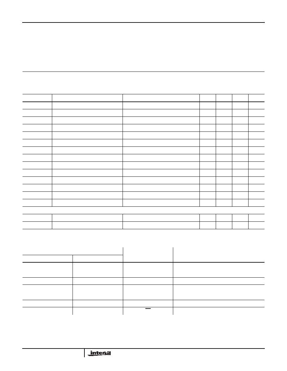
Absolute Maximum Ratings (TA = +25°C)
Thermal Information
Supply Voltage from VS+ to VS- . . . . . . . . . . . . . . . . . . . . . . . 13.2V
Slewrate between VS+ and VS-. . . . . . . . . . . . . . . . . . . . . . . . 1V/s
IIN-, IIN+, CE . . . . . . . . . . . . . . . . . . . . . . . . . . . . . . . . . . . . . . ±5mA
Continuous Output Current . . . . . . . . . . . . . . . . . . . . . . . . . . . 20mA
Storage Temperature . . . . . . . . . . . . . . . . . . . . . . . . -65°C to +150°C
Ambient Operating Temperature . . . . . . . . . . . . . . . -55°C to +125°C
Operating Junction Temperature . . . . . . . . . . . . . . . . . . . . . . +150°C
Power Dissipation . . . . . . . . . . . . . . . . . . . . . . . . . . . . . . . . . 192mW
CAUTION: Stresses above those listed in “Absolute Maximum Ratings” may cause permanent damage to the device. This is a stress only rating and operation of the
device at these or any other conditions above those indicated in the operational sections of this specification is not implied.
IMPORTANT NOTE: All parameters having Min/Max specifications are guaranteed. Typical values are for information purposes only. Unless otherwise noted, all tests
are at the specified temperature and are pulsed tests, therefore: TJ = TC = TA
Electrical Specifications
VS+ = +5V, VS- = -5V, RL = 500Ω, RF = 10kΩ, RG = 100Ω, TA = +25°C, unless otherwise specified.
PARAMETER
DESCRIPTION
CONDITIONS
MIN
TYP
MAX
UNIT
RIN
Input Resistance
Common mode
5
M
Ω
CIN
Input Capacitance
2pF
BW
-3dB Bandwidth
RF = 225Ω, AV = +10, RL = 1kΩ
670
MHz
BW
±0.1dB Bandwidth
RF = 225Ω, AV = +10, RL = 1kΩ
90
MHz
GBWP
Gain Bandwidth Product
3000
MHz
PM
Phase Margin
RL = 1kΩ, CL = 6pF
55
°
SR
Slew Rate
RL = 100Ω, VOUT = ±2.5V
1000
V/s
tR, tF
Rise Time, Fall Time
±0.1VSTEP
2.0
ns
OS
Overshoot
±0.1VSTEP
10
%
tS
0.01% Settling Time
6.6
ns
dG
Differential Gain
RF = 1kΩ, RLOAD = 150Ω
0.01
%
dP
Differential Phase
RF = 1kΩ, RLOAD = 150Ω
0.01
°
eN
Input Noise Voltage
f = 10kHz
0.9
nV/
√Hz
iN
Input Noise Current
f = 10kHz
3.5
pA/
√Hz
ENABLE (5962-0623601QPC Only)
tEN
Enable Time
220
nS
tDIS
Disable Time
175
nS
Pin Descriptions
PART
PIN NAME
FUNCTION
5962-0623601QPC
5962-0623602QPC
1, 5
1, 5, 8
NC
Not connected
2
IN-
Inverting input
3
IN+
Non-inverting input
4
VS-
Negative power supply
6
OUT
Amplifier output
7
VS+
Positive power supply
8CE
Enable and disable input
5962-0623601QPC, 5962-0623602QPC
相關(guān)PDF資料 |
PDF描述 |
|---|---|
| 5962-0623602QPX | 1 CHANNEL, AUDIO AMPLIFIER, CDIP8 |
| 5962-0623601QPX | 1 CHANNEL, AUDIO AMPLIFIER, CDIP8 |
| 5962-0623602QPX | 1 CHANNEL, AUDIO AMPLIFIER, CDIP8 |
| 5962-0625501QHX | 1 CHANNEL, VIDEO AMPLIFIER, CDFP10 |
| 5962-0625501QHX | 1 CHANNEL, VIDEO AMPLIFIER, CDFP10 |
相關(guān)代理商/技術(shù)參數(shù) |
參數(shù)描述 |
|---|---|
| 5962-0623602QPC | 制造商:Intersil Corporation 功能描述:OP AMP SGL VOLT FDBK 6V/12V 8PIN SBCDIP - Rail/Tube |
| 5962-0625501QHC | 制造商:Rochester Electronics LLC 功能描述: 制造商:Intersil Corporation 功能描述: |
| 5962-0625501QXC | 制造商:INTERSIL 制造商全稱:Intersil Corporation 功能描述:350MHz Fixed Gain Amplifiers with Enable |
| 5962-0625601QXC | 制造商:INTERSIL 制造商全稱:Intersil Corporation 功能描述:1.4GHz Current Feedback Amplifiers with Enable |
| 5962-0625602QXC | 制造商:INTERSIL 制造商全稱:Intersil Corporation 功能描述:1.4GHz Current Feedback Amplifiers with Enable |
發(fā)布緊急采購(gòu),3分鐘左右您將得到回復(fù)。