- 您現在的位置:買賣IC網 > PDF目錄68792 > 5962-0722201VFA (TEXAS INSTRUMENTS INC) OP-AMP, 5500 uV OFFSET-MAX, 3000 MHz BAND WIDTH, CDFP16 PDF資料下載
參數資料
| 型號: | 5962-0722201VFA |
| 廠商: | TEXAS INSTRUMENTS INC |
| 元件分類: | 運算放大器 |
| 英文描述: | OP-AMP, 5500 uV OFFSET-MAX, 3000 MHz BAND WIDTH, CDFP16 |
| 封裝: | CERAMIC, DFP-16 |
| 文件頁數: | 5/24頁 |
| 文件大小: | 840K |
| 代理商: | 5962-0722201VFA |
www.ti.com
TEST CIRCUITS
OutputMeasured
HereWithHigh-
Impedance
DifferentialProbe
THS4511
CM
VIN
RF
RG
RIT
From
50 W
Source
5V
49.9 W
100 W
0.22 F
m
49.9 W
0.22 F
m
Open
Distortion
Frequency Response
THS4511
CM
From
50 W
Source
VIN
0.22 F
m
49.9 W
VOUT
Open
To50 W
Test
Equipment
RG
RIT
RG
RIT
RF
5V
RO
ROT
0.22 F
m
1:1
RF
Slew Rate, Transient Response, Settling Time,
SLOS538A – SEPTEMBER 2007 – REVISED OCTOBER 2007
The
output
is
probed
using
a
high-impedance
differential probe across the 100
resistor. The gain
The THS4511 is tested with the following test circuits.
is referred to the amplifier output by adding back the
For simplicity, the power supply decoupling is not
6 dB loss due to the voltage divider on the output.
shown – see the layout in the application information
section for recommendations. Depending on the test
conditions, component values are changed per the
following tables, or as otherwise noted. The signal
generators used are ac coupled 50
sources, and a
0.22
μF capacitor and a 49.9 resistor to ground are
inserted across RIT on the alternate input to balance
the circuit.
Table 1. Gain Component Values
GAIN
RF
RG
RIT
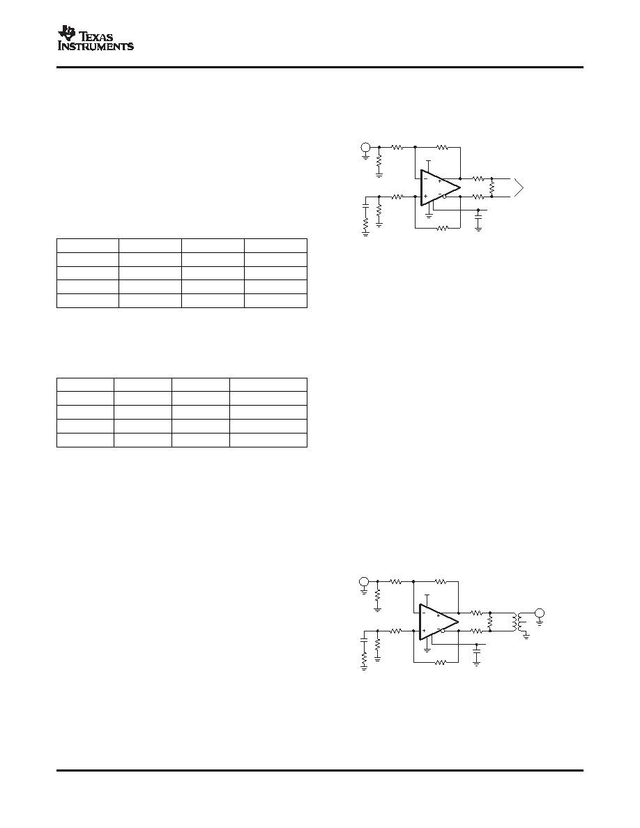
Figure 30. Frequency Response Test Circuit
6 dB
348
165
61.9
10 dB
348
100
69.8
14 dB
348
56.2
88.7
20 dB
348
16.5
287
The circuit shown in Figure 31 is used to measure
harmonic distortion and intermodulation distortion of
Note: The gain setting includes 50
source
the amplifier.
impedance. Components are chosen to achieve
A signal generator is used as the signal source, and
gain and 50
input termination.
the output is measured with a spectrum analyzer. The
output impedance of the signal generator is 50
. RIT
Table 2. Load Component Values
and RG are chosen to impedance-match to 50 and
RL
RO
ROT
Atten
to maintain the proper gain. To balance the amplifier,
100
25
open
6 dB
a 0.22
μF capacitor and 49.9 resistor to ground are
200
86.6
69.8
16.8 dB
inserted across RIT on the alternate input.
499
237
56.2
25.5 dB
A low-pass filter is inserted in series with the input to
1k
487
52.3
31.8 dB
reduce harmonics generated at the signal source.
The level of the fundamental is measured, then a
Note: The total load includes 50
termination by
high-pass filter is inserted at the output to reduce the
the test equipment. Components are chosen to
fundamental so that it does not generate distortion in
achieve load and 50
line termination through a
the input of the spectrum analyzer.
1:1 transformer.
The transformer used in the output to convert the
Due to the voltage divider on the output formed by
signal
from
differential
to
single
ended
is
an
the load component values, the amplifier's output is
ADT1-1WT. It limits the frequency response of the
attenuated. The column Atten in Table 2 shows the
circuit so that measurements cannot be made below
attenuation expected from the resistor divider. When
approximately 1 MHz.
using a transformer at the output as shown in
Figure 31, the signal will see slightly more loss, and
these numbers will be approximate.
The circuit shown in Figure 30 is used to measure the
frequency response of the circuit.
A network analyzer is used as the signal source and
as the measurement device. The output impedance
of the network analyzer is 50
. RIT and RG are
chosen to impedance match to 50
, and to maintain
Figure 31. Distortion Test Circuit
the proper gain. To balance the amplifier, a 0.22
μF
capacitor and 49.9
resistor to ground are inserted
across RIT on the alternate input.
Output Impedance, Overdrive, Output Voltage,
Copyright 2007, Texas Instruments Incorporated
13
Product Folder Link(s): THS4511–SP
相關PDF資料 |
PDF描述 |
|---|---|
| 5962-554901NXDR | DUAL COMPARATOR, 10000 uV OFFSET-MAX, 650 ns RESPONSE TIME, PDSO8 |
| 5962-751401QHA | DUAL OP-AMP, 2500 uV OFFSET-MAX, 0.046 MHz BAND WIDTH, CDFP10 |
| 5962-8760401GA | OP-AMP, 3000 uV OFFSET-MAX, MBCY8 |
| 5962-8760601GX | BUFFER AMPLIFIER, MBCY8 |
| 5962-8760601CX | BUFFER AMPLIFIER, CDIP14 |
相關代理商/技術參數 |
參數描述 |
|---|---|
| 5962-0722301VFA | 制造商:Texas Instruments 功能描述:SP Amp DIFF AMP Single ±2.5V/5V 16-Pin CFPAK Tube 制造商:Rochester Electronics LLC 功能描述: 制造商:Texas Instruments 功能描述:MIL SPEC TI IC PART |
| 5962-0722401QXB | 制造商:ATMEL 制造商全稱:ATMEL Corporation 功能描述:Rad-Hard 32 bit SPARC V8 Processor |
| 5962-0722901QXA | 功能描述:線性穩壓器 - 標準 RoHS:否 制造商:STMicroelectronics 輸出類型: 極性: 輸出電壓:1.8 V 輸出電流:150 mA 負載調節: 最大輸入電壓:5.5 V 線路調整率: 最大工作溫度:+ 125 C 安裝風格:SMD/SMT 封裝 / 箱體:SOT-323-5L |
| 5962-0722902QZA | 制造商:Texas Instruments 功能描述:MICROCIRCUIT, VOLTAGE REGULATOR - Rail/Tube |
| 5962-0723001VXC | 制造商:Texas Instruments 功能描述:HIGH PERFORMANCE CLOCK SYNC - Rail/Tube |
發布緊急采購,3分鐘左右您將得到回復。