- 您現(xiàn)在的位置:買賣IC網(wǎng) > PDF目錄91412 > 5962-8870101UA (MS KENNEDY CORP) OP-AMP, 1000 uV OFFSET-MAX, DFM8 PDF資料下載
參數(shù)資料
| 型號: | 5962-8870101UA |
| 廠商: | MS KENNEDY CORP |
| 元件分類: | 運算放大器 |
| 英文描述: | OP-AMP, 1000 uV OFFSET-MAX, DFM8 |
| 封裝: | POWER, Z-TAB PACKAGE-8 |
| 文件頁數(shù): | 2/7頁 |
| 文件大小: | 482K |
| 代理商: | 5962-8870101UA |
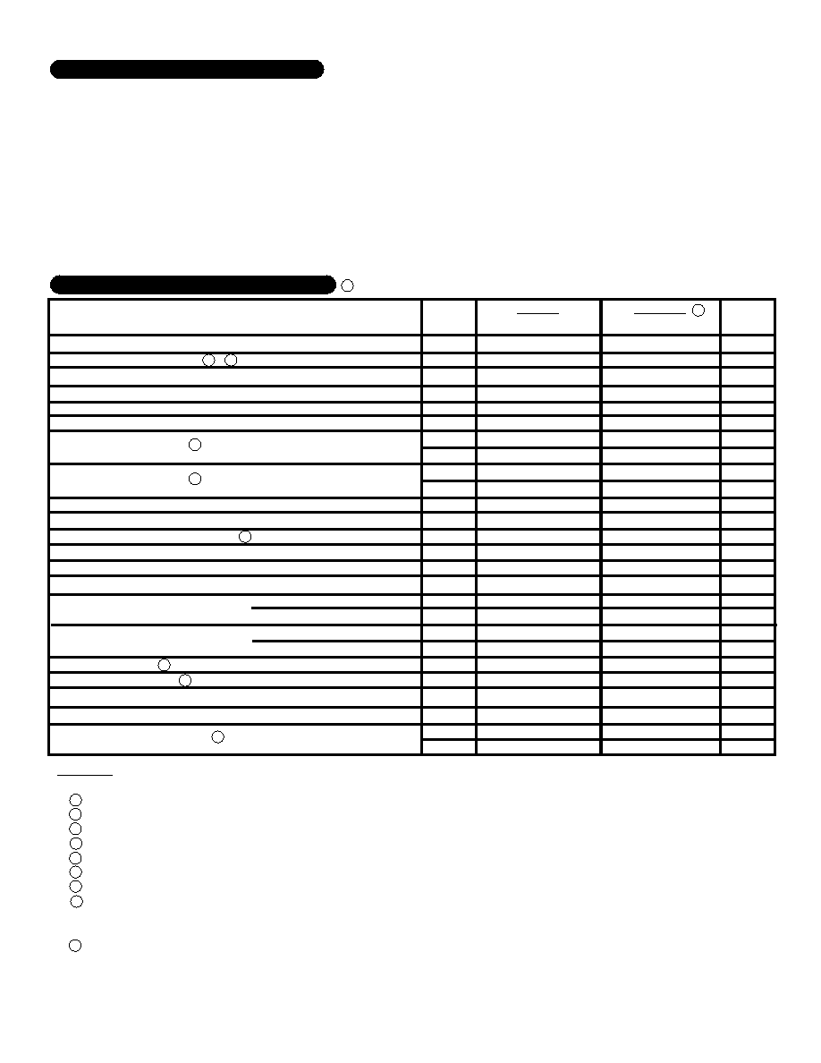
Group A
Subgroup
-
1,2,3
1
2,3
1
2,3
1
2,3
-
4
5,6
4
5,6
-
4
5,6
STATIC
Supply Voltage Range
Quiescent Current
INPUT
Input Offset Voltage
Input Offset Voltage Drift
Input Capacitance
Input Impedance
Common Mode Rejection Ratio
Power Supply Rejection Ratio
Input Noise Voltage
OUTPUT
Settling Time
Power Bandwidth
TRANSFER CHARACTERISTICS
Slew Rate
Max.
±40
±35
±10
-
±100
-
30
-
Typ.
±35
±20
±1.0
±15
±4
±0.2
2.0
-
5
1012
113
90
10
±29
-
±8
-
2
50
10
100
-
Min.
±10
-
90
-
±28
-
±5
-
40
6
90
-
Max.
±40
±30
±1.0
±50
±10
30
20
-
Typ.
±35
±20
±0.1
±15
±4
±0.2
2.0
-
5
1012
113
90
10
±29
±31
±8
-
2
55
10
100
-
Min.
±10
-
95
-
±28
±30
±5
±3.0
-
45
6
95
85
VIN = 0V
VCM = 0V
Either Input
F = DC
F = DC VCM = ±22V
VCC = ±10V to ±40V
F = 10 Hz to 1 KHz
RL = 5.6 F = 10 KHz
RL =10
F = 10 KHz
RL = 5.6 F =10 KHz
RL = 10 F = 10 KHz
0.1% 2V step
RL = 10 VO = 20 VRMS
VOUT = ±10V RL = 10
±VCC Supply Voltage
±40V
IOUT
Peak Output Current
See S.O.A.
VIN
Differential Input Voltage
±VCC
VIN
Common Mode Input Voltage
±VCC
RTH
Thermal Resistance-Junction to Case
MSK 541
1.9° C/W
MSK 145
1.2° C/W
MSK 146
1.2° C/W
MSK 147
1.2° C/W
ABSOLUTE MAXIMUM RATINGS
ELECTRICAL SPECIFICATIONS
TST
Storage Temperature Range
-65° to +150°C
TLD
Lead Temperature Range
300°
(10 Seconds)
PD
Power Dissipation
125W
TJ
Junction Temperature
150°C
TC
Case Operating Temperature Range
Military Versions
-55°C to +125°C
Industrial Versions
-40°C to +85°C
Units
V
mA
mV
V/°C
pA
nA
pA
nA
pF
W
dB
VRMS
V
A
S
KHz
V/S
dB
NOTES:
1
Unless otherwise specified RCL = 0, ±VCC = ±34 VDC
2
Electrical specifications are derated for power supply voltages other than ±34 VDC.
3
AV = -1, measured in false summing junction circuit.
4
Devices shall be capable of meeting the parameter, but need not be tested. Typical parameters are for reference only.
5
Industrial grade devices shall be tested to subgroups 1 and 4 unless otherwise specified.
6
Military grade devices ('B' suffix) shall be 100% tested to subgroups 1, 2, 3 and 4.
7
Subgroup 5 and 6 testing available upon request.
8
Subgroup 1, 4
TA = TC = +25°C
Subgroup 2, 5
TA = TC = +125°C
Subgroup 3, 6
TA = TC =
-55°C
Rereference DSCC SMD 5962-8870101 for electrical specifications for devices purchased as such.
3
4
2
Rev. C 3/01
Military
Industrial
2
4
VCM=0V
Input Offset Current
Input Bias Current
Output Voltage Swing
Output Current
Open Loop Voltage Gain
F = 10 HZ RL = 10 K
Parameter
Test Conditions
5
○○○○○○○
○○○○○○
○○○○○○○○
○○○○○○
○○○○○○○○
○○○○○○
○○○○○○○○
○
○○○○○○
○
○○○
○○○○○○○○
○
○○○○○○○○○○○
○
○○○○○○○○○○○
○
○○○○○○○○○
○
○○○○○○○○○○○○
○○○○○○○○
○○○○○○○○○
○
○○○○
○○○○○
○○○○○○○○○
9
4
9
相關PDF資料 |
PDF描述 |
|---|---|
| 5962-8870101UX | OP-AMP, 1000 uV OFFSET-MAX, MDFM8 |
| 5962-8870101XX | OP-AMP, 1000 uV OFFSET-MAX, MBFM8 |
| 5962-8870101YX | OP-AMP, 1000 uV OFFSET-MAX, MDIP8 |
| 5962-8870102XX | OP-AMP, 1000 uV OFFSET-MAX, MBFM8 |
| 5962-8870101UX | OP-AMP, 1000 uV OFFSET-MAX, DFM8 |
相關代理商/技術參數(shù) |
參數(shù)描述 |
|---|---|
| 5962-8870201RA | 制造商:QP Semiconductor 功能描述:AC377/C NSC DIE - DIP 制造商:Texas Instruments 功能描述:Flip Flop D-Type Bus Interface Pos-Edge 1-Element 20-Pin CDIP Rail |
| 5962-88703012A | 制造商:QP Semiconductor 功能描述:Multiplexer 1-Element CMOS 3-ST 8-IN 20-Pin CLLCC |
| 5962-8870301EA | 制造商:QP Semiconductor 功能描述:Multiplexer 1-Element CMOS 3-ST 8-IN 16-Pin CDIP |
| 5962-88705013A | 制造商:Texas Instruments 功能描述: |
| 5962-8870501KA | 制造商:QP Semiconductor 功能描述:Flip Flop D-Type Bus Interface Pos-Edge 3-ST 1-Element 24-Pin CPAK 制造商:Texas Instruments 功能描述:10-BIT D FLIP-FLOP WITH TRI-STATE OUTPUTS |
發(fā)布緊急采購,3分鐘左右您將得到回復。