- 您現在的位置:買賣IC網 > PDF目錄56729 > 5962-8948102VX (ANALOG DEVICES INC) PARALLEL, WORD INPUT LOADING, 0.6 us SETTLING TIME, 12-BIT DAC, CDIP18 PDF資料下載
參數資料
| 型號: | 5962-8948102VX |
| 廠商: | ANALOG DEVICES INC |
| 元件分類: | DAC |
| 英文描述: | PARALLEL, WORD INPUT LOADING, 0.6 us SETTLING TIME, 12-BIT DAC, CDIP18 |
| 封裝: | GLASS SEALED, CERDIP-18 |
| 文件頁數: | 4/9頁 |
| 文件大小: | 206K |
| 代理商: | 5962-8948102VX |
AD7541A
–4–
REV. B
GENERAL CIRCUIT INFORMATION
The simplified D/A circuit is shown in Figure 1. An inverted
R-2R ladder structure is used—that is, the binarily weighted
currents are switched between the OUT1 and OUT2 bus lines,
thus maintaining a constant current in each ladder leg indepen-
dent of the switch state.
10k
10k
10k
20k
20k
20k
20k
20k
S1
S2
S3
S12
VREF
OUT2
OUT1
RFEEDBACK
BIT 12 (LSB)
BIT 3
BIT 2
BIT 1 (MSB)
DIGITAL INPUTS (DTL/TTL/CMOS COMPATIBLE)
LOGIC: A SWITCH IS CLOSED TO IOUT1 FOR
ITS DIGITAL INPUT IN A "HIGH" STATE.
10k
Figure 1. Functional Diagram (Inputs HIGH)
The input resistance at VREF (Figure 1) is always equal to RLDR
(RLDR is the R/2R ladder characteristic resistance and is equal to
value “R”). Since RIN at the VREF pin is constant, the reference
terminal can be driven by a reference voltage or a reference
current, ac or dc, of positive or negative polarity. (If a current
source is used, a low temperature coefficient external RFB is
recommended to define scale factor.)
EQUIVALENT CIRCUIT ANALYSIS
The equivalent circuits for all digital inputs LOW and all digital
inputs HIGH are shown in Figures 2 and 3. In Figure 2 with all
digital inputs LOW, the reference current is switched to OUT2.
The current source ILEAKAGE is composed of surface and junc-
tion leakages to the substrate, while the I/4096 current source
represents a constant 1-bit current drain through the termina-
tion resistor on the R-2R ladder. The ON capacitance of the
output N-channel switch is 200 pF, as shown on the OUT2
terminal. The OFF switch capacitance is 70 pF, as shown on
the OUT1 terminal. Analysis of the circuit for all digital inputs
HIGH, as shown in Figure 3 is similar to Figure 2; however, the
ON switches are now on terminal OUT1, hence the 200 pF at
that terminal.
ILEAKAGE
70pF
R
ILEAKAGE
200pF
I/4096
IREF
R
15k
VREF
RFB
OUT1
OUT2
Figure 2. DAC Equivalent Circuit All Digital Inputs LOW
ILEAKAGE
70pF
R
ILEAKAGE
200pF
I/4096
IREF
R
15k
VREF
RFB
OUT2
OUT1
Figure 3. DAC Equivalent Circuit All Digital Inputs HIGH
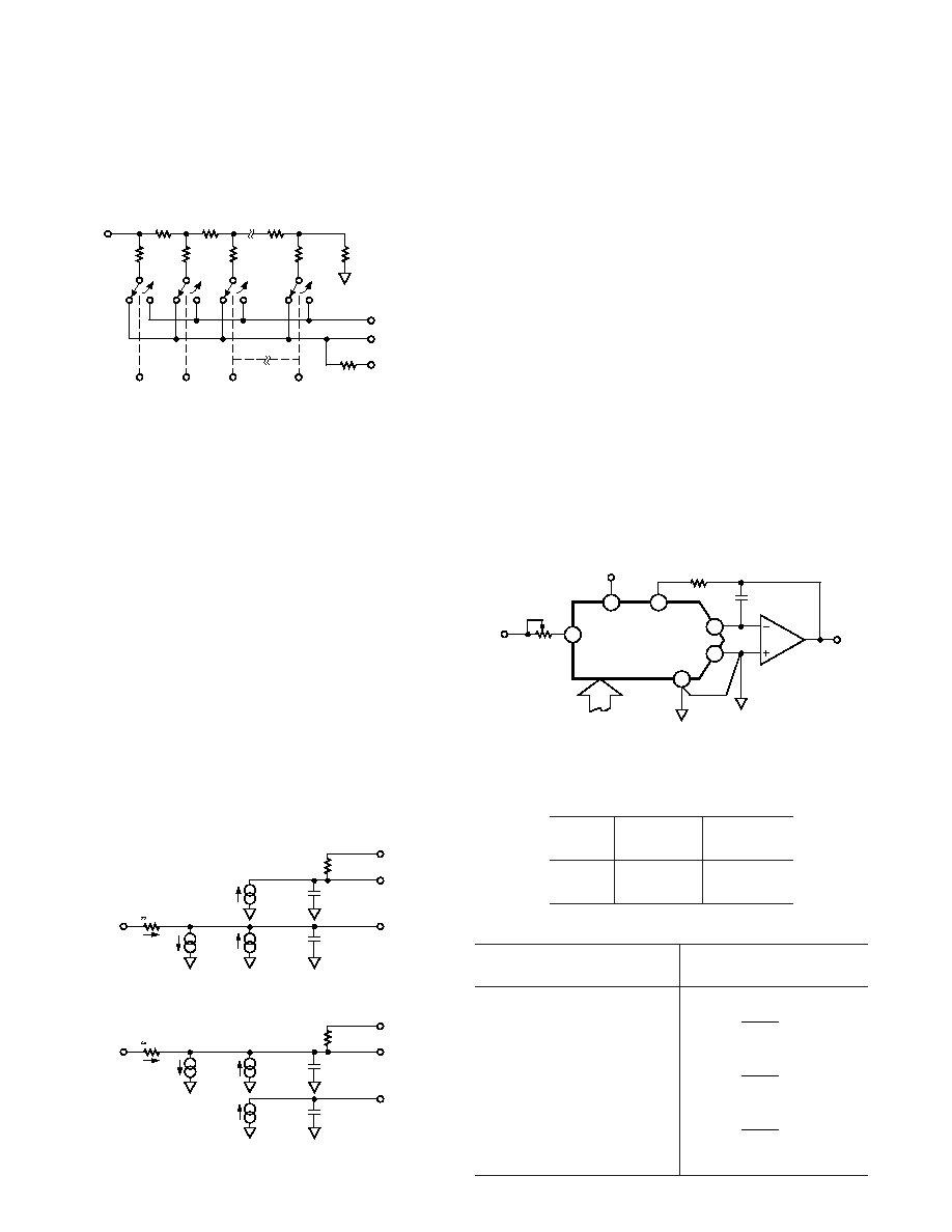
APPLICATIONS
UNIPOLAR BINARY OPERATION
(2-QUADRANT MULTIPLICATION)
Figure 4 shows the analog circuit connections required for uni-
polar binary (2-quadrant multiplication) operation. With a dc
reference voltage or current (positive or negative polarity) ap-
plied at Pin 17, the circuit is a unipolar D/A converter. With an
ac reference voltage or current, the circuit provides 2-quadrant
multiplication (digitally controlled attenuation). The input/
output relationship is shown in Table II.
R1 provides full-scale trim capability [i.e., load the DAC register
to 1111 1111 1111, adjust R1 for VOUT = –VREF (4095/4096)].
Alternatively, Full Scale can be adjusted by omitting R1 and R2
and trimming the reference voltage magnitude.
C1 phase compensation (10 pF to 25 pF) may be required for
stability when using high speed amplifiers. (C1 is used to cancel
the pole formed by the DAC internal feedback resistance and
output capacitance at OUT1).
Amplifier A1 should be selected or trimmed to provide VOS
≤
10% of the voltage resolution at VOUT. Additionally, the ampli-
fier should exhibit a bias current which is low over the tempera-
ture range of interest (bias current causes output offset at VOUT
equal to IB times the DAC feedback resistance, nominally 11 k
).
The AD544L is a high speed implanted FET input op amp with
low factory-trimmed VOS.
18
16
1
2
3
17
AD7541A
VDD
RFB
VDD
VREF
PINS 4–15
DGND
OUT1
OUT2
R1
*
VIN
BIT 1 – BIT 12
DIGITAL
GROUND
ANALOG
COMMON
R2
*
C1
33pF
AD544L
(SEE TEXT)
VOUT
*REFER TO TABLE 1
Figure 4. Unipolar Binary Operation
Table I. Recommended Trim Resistor Values vs. Grades
Trim
Resistor
JN/AQ/SD
KN/BQ/TD
R1
100
100
R2
47
33
Table II. Unipolar Binary Code Table for Circuit of Figure 4
Binary Number in DAC
MSB
LSB
Analog Output, VOUT
1 1 1 1
–VIN
4095
4096
1 0 0 0
0 0 0 0
–VIN
2048
4096
= –1/2 VIN
0 0 0 0
0 0 0 1
–VIN
1
4096
0 0 0 0
0 Volts
相關PDF資料 |
PDF描述 |
|---|---|
| 5962-8949907XC | SYNCHRO OR RESOLVER TO DIGITAL CONVERTER, DIP36 |
| 5962-8949908XC | SYNCHRO OR RESOLVER TO DIGITAL CONVERTER, DIP36 |
| 5962-8990812XC | SYNCHRO OR RESOLVER TO DIGITAL CONVERTER, DIP36 |
| 5962-8990813XC | SYNCHRO OR RESOLVER TO DIGITAL CONVERTER, DIP36 |
| 5962-8990811XC | SYNCHRO OR RESOLVER TO DIGITAL CONVERTER, DIP36 |
相關代理商/技術參數 |
參數描述 |
|---|---|
| 5962-89481032A | 制造商:Rochester Electronics LLC 功能描述:- Bulk |
| 5962-8948103VA | 制造商:Rochester Electronics LLC 功能描述:- Bulk |
| 5962-8948104VA | 制造商:Rochester Electronics LLC 功能描述:12-BIT MULTIPLYING DAC IC - Bulk |
| 5962-8948401M3A | 制造商:QP Semiconductor 功能描述:EPROM UV 64K-Bit 8K x 8 50ns 28-Pin LLCC |
| 5962-8948403MXA | 制造商:QP Semiconductor 功能描述:EPROM UV 64K-Bit 8K x 8 15ns 28-Pin CDIP |
發布緊急采購,3分鐘左右您將得到回復。