- 您現在的位置:買賣IC網 > PDF目錄97782 > 5962-8949404PA (TEXAS INSTRUMENTS INC) DUAL OP-AMP, 3750 uV OFFSET-MAX, 0.14 MHz BAND WIDTH, CDIP8 PDF資料下載
參數資料
| 型號: | 5962-8949404PA |
| 廠商: | TEXAS INSTRUMENTS INC |
| 元件分類: | 運算放大器 |
| 英文描述: | DUAL OP-AMP, 3750 uV OFFSET-MAX, 0.14 MHz BAND WIDTH, CDIP8 |
| 封裝: | CERAMIC, DIP-8 |
| 文件頁數: | 1/46頁 |
| 文件大小: | 1011K |
| 代理商: | 5962-8949404PA |
當前第1頁第2頁第3頁第4頁第5頁第6頁第7頁第8頁第9頁第10頁第11頁第12頁第13頁第14頁第15頁第16頁第17頁第18頁第19頁第20頁第21頁第22頁第23頁第24頁第25頁第26頁第27頁第28頁第29頁第30頁第31頁第32頁第33頁第34頁第35頁第36頁第37頁第38頁第39頁第40頁第41頁第42頁第43頁第44頁第45頁第46頁
TLC27L2, TLC27L2A, TLC27L2B, TLC27L7
LinCMOS PRECISION DUAL OPERATIONAL AMPLIFIERS
SLOS052D OCTOBER 1987 REVISED OCTOBER 2005
1
POST OFFICE BOX 655303
DALLAS, TEXAS 75265
D Trimmed Offset Voltage:
TLC27L7 . . . 500
V Max at 25°C,
VDD = 5 V
D Input Offset Voltage Drift . . . Typically
0.1
V/Month, Including the First 30 Days
D Wide Range of Supply Voltages Over
Specified Temperature Range:
0
°C to 70°C...3 V to 16 V
40
°C to 85°C...4 V to 16 V
55
°C to 125°C...4 V to 16 V
D Single-Supply Operation
D Common-Mode Input Voltage Range
Extends Below the Negative Rail (C-Suffix,
I-Suffix Types)
D Ultra-Low Power ...Typically 95 W
at 25
°C, VDD = 5 V
D Output Voltage Range Includes Negative
Rail
D High Input Impedance ...1012 Typ
D ESD-Protection Circuitry
D Small-Outline Package Option Also
Available in Tape and Reel
D Designed-In Latch-Up immunity
description
The TLC27L2 and TLC27L7 dual operational
amplifiers combine a wide range of input offset
voltage grades with low offset voltage drift, high
input impedance, extremely low power, and high
gain.
AVAILABLE OPTIONS
PACKAGE
TA
VIOmax
AT 25
°C
SMALL
OUTLINE
(D)
CHIP
CARRIER
(FK)
CERAMIC
DIP
(JG)
PLASTIC
DIP
(P)
0
°C
500
V TLC27L7CD
TLC27L7CP
0
°C
to
500
V
2 mV
TLC27L7CD
TLC27L2BCD
—
TLC27L7CP
TLC27L2BCP
to
70
°C
2 mV
5 mV
TLC27L2BCD
TLC27L2ACD
—
TLC27L2BCP
TLC27L2ACP
70
°C
5 mV
10 mV
TLC27L2ACD
TLC27L2CD
TLC27L2ACP
TLC27L2CP
40
°C
500
V TLC27L7ID
TLC27L7IP
40
°C
to
500
V
2 mV
TLC27L7ID
TLC27L2BID
—
TLC27L7IP
TLC27L2BIP
to
85
°C
2 mV
5 mV
TLC27L2BID
TLC27L2AID
—
TLC27L2BIP
TLC27L2AIP
85
°C
5 mV
10 mV
TLC27L2AID
TLC27L2ID
TLC27L2AIP
TLC27L2IP
55
°C
to
500
V
TLC27L7MD
TLC27L2MD
TLC27L7MFK
TLC27L7MJG
TLC27L7MP
to
125
°C
500
V
10 mV
TLC27L2MD
TLC27L2MDRG4
TLC27L7MFK
TLC27L2MFK
TLC27L7MJG
TLC27L2MJG
TLC27L7MP
TLC27L2MP
The D package is available taped and reeled. Add R suffix to the device type
(e.g., TLC27L7CDR).
Copyright
2005, Texas Instruments Incorporated
PRODUCTION DATA information is current as of publication date.
Products conform to specifications per the terms of Texas Instruments
standard warranty. Production processing does not necessarily include
testing of all parameters.
LinCMOS is a trademark of Texas Instruments.
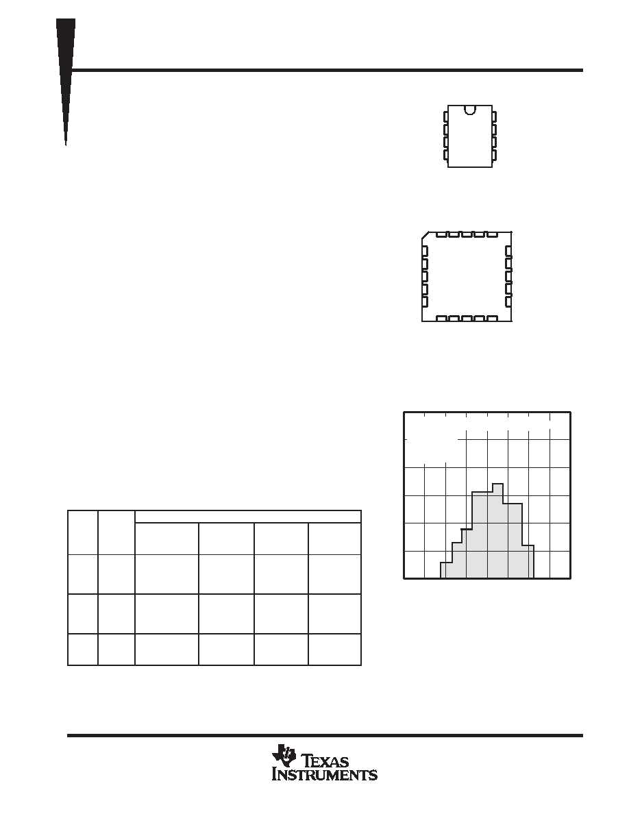
800
Percentage
of
Units
%
VIO Input Offset Voltage V
30
800
0
400
0
400
5
10
15
20
25
DISTRIBUTION OF TLC27L7
INPUT OFFSET VOLTAGE
1
2
3
4
8
7
6
5
1OUT
1IN
1IN +
GND
VDD
2OUT
2IN
2IN +
D, JG, OR P PACKAGE
(TOP VIEW)
3
2
1 20 19
910 11 12 13
4
5
6
7
8
18
17
16
15
14
NC
2OUT
NC
2IN
NC
1IN
NC
1IN +
NC
FK PACKAGE
(TOP VIEW)
NC
1OUT
NC
GND
NC
NC No internal connection
2IN
+
DD
V
335 Units Tested From 2 Wafer Lots
VDD = 5 V
TA = 25°C
P Package
相關PDF資料 |
PDF描述 |
|---|---|
| 5962-89621012HA | OP-AMP, 10000 uV OFFSET-MAX, 50 MHz BAND WIDTH, CDFP10 |
| 5962-89621012PA | OP-AMP, 10000 uV OFFSET-MAX, 50 MHz BAND WIDTH, CDIP8 |
| 5962-89621012VPA | OP-AMP, 10000 uV OFFSET-MAX, 50 MHz BAND WIDTH, CDIP8 |
| 5962-89621012VXA | OP-AMP, 10000 uV OFFSET-MAX, 50 MHz BAND WIDTH, CDSO10 |
| 5962-89621012XA | OP-AMP, 10000 uV OFFSET-MAX, 50 MHz BAND WIDTH, CDSO10 |
相關代理商/技術參數 |
參數描述 |
|---|---|
| 5962-8949703MXA | 制造商:Micross Components, Inc. 功能描述:256KX4 VRAM 400 MIL DIP - Tape and Reel |
| 5962-89502012A | 制造商:Rochester Electronics LLC 功能描述:- Bulk |
| 5962-8950201GC | 制造商:Intersil Corporation 功能描述:OP AMP SGL GP 15V 8PDIP - Bulk 制造商:Rochester Electronics LLC 功能描述:- Bulk |
| 5962-89503012A | 制造商:Texas Instruments 功能描述:Standard Timer Single 20-Pin LCCC Tube 制造商:Rochester Electronics LLC 功能描述:- Bulk 制造商:Texas Instruments 功能描述:STD TIMER SGL 20LCCC - Rail/Tube |
| 5962-8950301PA | 制造商:Texas Instruments 功能描述:Standard Timer Single 8-Pin CDIP Tube 制造商:Texas Instruments 功能描述:STD TIMER SGL 8CDIP - Rail/Tube |
發布緊急采購,3分鐘左右您將得到回復。