- 您現在的位置:買賣IC網 > PDF目錄68796 > 5962-90604042A (TEXAS INSTRUMENTS INC) QUAD OP-AMP, 3750 uV OFFSET-MAX, 0.525 MHz BAND WIDTH, CQCC20 PDF資料下載
參數資料
| 型號: | 5962-90604042A |
| 廠商: | TEXAS INSTRUMENTS INC |
| 元件分類: | 運算放大器 |
| 英文描述: | QUAD OP-AMP, 3750 uV OFFSET-MAX, 0.525 MHz BAND WIDTH, CQCC20 |
| 封裝: | CERAMIC, LCC-20 |
| 文件頁數: | 2/43頁 |
| 文件大小: | 762K |
| 代理商: | 5962-90604042A |
第1頁當前第2頁第3頁第4頁第5頁第6頁第7頁第8頁第9頁第10頁第11頁第12頁第13頁第14頁第15頁第16頁第17頁第18頁第19頁第20頁第21頁第22頁第23頁第24頁第25頁第26頁第27頁第28頁第29頁第30頁第31頁第32頁第33頁第34頁第35頁第36頁第37頁第38頁第39頁第40頁第41頁第42頁第43頁
TLC27M4, TLC27M4A, TLC27M4B, TLC27M4Y, TLC27M9
LinCMOS
PRECISION QUAD OPERATIONAL AMPLIFIERS
SLOS093C – OCTOBER 1987 – REVISED MAY 1999
10
POST OFFICE BOX 655303
DALLAS, TEXAS 75265
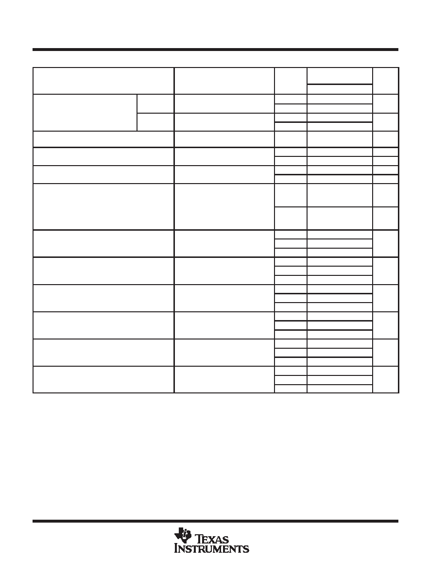
electrical characteristics at specified free-air temperature, VDD = 5 V (unless otherwise noted)
PARAMETER
TEST CONDITIONS
TA
TLC27M4M
TLC27M9M
UNIT
TA
MIN
TYP
MAX
TLC27M4M
VO = 1.4 V,
VIC = 0,
25
°C
1.1
10
mV
VIO
Input offset voltage
TLC27M4M
O
,
RS = 50 ,
IC
,
RL = 100 k
Full range
12
mV
VIO
Input offset voltage
TLC27M9M
VO = 1.4 V,
VIC = 0,
25
°C
210
900
V
TLC27M9M
O
,
RS = 50 ,
IC
,
RL = 100 k
Full range
3750
V
αVIO
Average temperature coefficient of input
offset voltage
25
°C to
125
°C
1.7
V/°C
IIO
Input offset current (see Note 4)
VO =2 5V
VIC =2 5V
25
°C
0.1
pA
IIO
Input offset current (see Note 4)
VO = 2.5 V,
VIC = 2.5 V
125
°C
1.4
15
nA
IIB
Input bias current (see Note 4)
VO =2 5V
VIC =2 5V
25
°C
0.6
pA
IIB
Input bias current (see Note 4)
VO = 2.5 V,
VIC = 2.5 V
125
°C
9
35
nA
VICR
Common-mode input voltage range
25
°C
0
to
4
– 0.3
to
4.2
V
VICR
gg
(see Note 5)
Full range
0
to
3.5
V
25
°C
3.2
3.9
VOH
High-level output voltage
VID = 100 mV,
RL = 100 k
–55
°C
3
3.9
V
125
°C
3
4
25
°C
0
50
VOL
Low-level output voltage
VID = – 100 mV,
IOL = 0
– 55
°C
0
50
mV
125
°C
0
50
Large signal differential
25
°C
25
170
AVD
Large-signal differential
voltage amplification
VO = 0.25 V to 2 V,
RL = 100 k
–55
°C
15
290
V/mV
voltage am lification
125
°C
15
120
25
°C
65
91
CMRR
Common-mode rejection ratio
VIC = VICRmin
–55
°C
60
89
dB
125
°C
60
91
Supply voltage rejection ratio
25
°C
70
93
kSVR
Supply-voltage rejection ratio
(
VDD/VIO)
VDD = 5 V to 10 V,
VO = 1.4 V
– 55
°C
60
91
dB
(
VDD/VIO)
125
°C
60
94
V2 5 V
25
°C
420
1120
IDD
Supply current (four amplifiers)
VO = 2.5 V,
No load
VIC = 2.5 V,
–55
°C
680
1760
A
No load
125
°C
280
720
Full range is – 55
°C to 125°C.
NOTES:
4. The typical values of input bias current and input offset current below 5 pA were determined mathematically.
5. This range also applies to each input individually.
相關PDF資料 |
PDF描述 |
|---|---|
| 5962-9081201MGA | BUFFER AMPLIFIER, MBCY8 |
| 5962-9081201MPA | BUFFER AMPLIFIER, CDIP8 |
| 5962-9088102M2A | DUAL OP-AMP, 700 uV OFFSET-MAX, 2.8 MHz BAND WIDTH, CQCC20 |
| 5962-9088102MPA | DUAL OP-AMP, 700 uV OFFSET-MAX, 2.8 MHz BAND WIDTH, CDIP8 |
| 5962-9088105Q2A | DUAL OP-AMP, 450 uV OFFSET-MAX, 2.8 MHz BAND WIDTH, CQCC20 |
相關代理商/技術參數 |
參數描述 |
|---|---|
| 5962-9060404CA | 制造商:Rochester Electronics LLC 功能描述:- Bulk |
| 5962-90604052A | 制造商:Rochester Electronics LLC 功能描述:- Bulk |
| 5962-90606022A | 制造商:e2v Aerospace & Defense 功能描述:SMD MKD 54F112 LCC FSC |
| 5962-9060602EA | 制造商:e2v Aerospace & Defense 功能描述:SMD MKD 54F112 FSC-DIP |
| 5962-9060602FA | 制造商:e2v Aerospace & Defense 功能描述:SMD MKD 54F112 FP-FSC |
發布緊急采購,3分鐘左右您將得到回復。