- 您現在的位置:買賣IC網 > PDF目錄68796 > 5962-9088204Q2A (TEXAS INSTRUMENTS INC) DUAL OP-AMP, 750 uV OFFSET-MAX, 1.9 MHz BAND WIDTH, CQCC20 PDF資料下載
參數資料
| 型號: | 5962-9088204Q2A |
| 廠商: | TEXAS INSTRUMENTS INC |
| 元件分類: | 運算放大器 |
| 英文描述: | DUAL OP-AMP, 750 uV OFFSET-MAX, 1.9 MHz BAND WIDTH, CQCC20 |
| 封裝: | CERAMIC, LCC-20 |
| 文件頁數: | 7/67頁 |
| 文件大小: | 1352K |
| 代理商: | 5962-9088204Q2A |
第1頁第2頁第3頁第4頁第5頁第6頁當前第7頁第8頁第9頁第10頁第11頁第12頁第13頁第14頁第15頁第16頁第17頁第18頁第19頁第20頁第21頁第22頁第23頁第24頁第25頁第26頁第27頁第28頁第29頁第30頁第31頁第32頁第33頁第34頁第35頁第36頁第37頁第38頁第39頁第40頁第41頁第42頁第43頁第44頁第45頁第46頁第47頁第48頁第49頁第50頁第51頁第52頁第53頁第54頁第55頁第56頁第57頁第58頁第59頁第60頁第61頁第62頁第63頁第64頁第65頁第66頁第67頁
TLC220x, TLC220xA, TLC220xB, TLC220xY
Advanced LinCMOS LOW NOISE PRECISION
OPERATIONAL AMPLIFIERS
SLOS175B FEBRUARY 1997 REVISED JANUARY 2008
15
POST OFFICE BOX 655303
DALLAS, TEXAS 75265
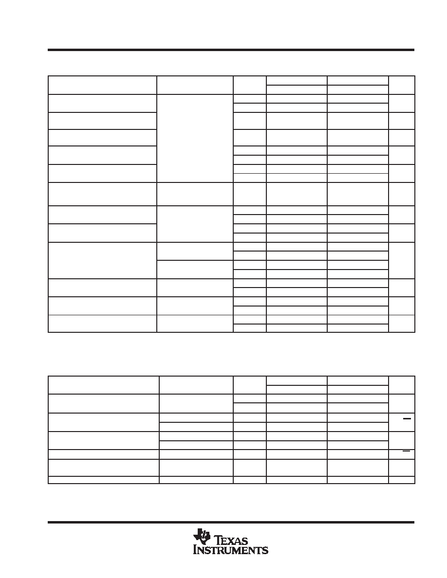
TLC2202C electrical characteristics at specified free-air temperature, VDD± = ±5 V (unless
otherwise noted)
PARAMETER
TEST CONDITIONS
TA
TLC2202AC
TLC2202BC
UNIT
PARAMETER
TEST CONDITIONS
TA
MIN
TYP
MAX
MIN
TYP
MAX
UNIT
VIO
Input offset voltage
25
°C
80
500
80
500
V
VIO
Input offset voltage
Full range
650
V
αVIO
Temperature coefficient
of input offset voltage
Full range
0.5
V/°C
αVIO
Temperature coefficient
of input offset voltage
Full range
0.5
V/°C
Input offset voltage long-term
drift (see Note 4)
VIC = 0,
RS = 50
25
°C
0.001
0.005
0.001
0.005
V/mo
IIO
Input offset current
25
°C
0.5
60
0.5
60
pA
IIO
Input offset current
Full range
100
pA
IIB
Input bias current
25
°C
1
60
1
60
pA
IIB
Input bias current
Full range
100
pA
Common-mode input voltage
5
VICR
Common-mode input voltage
range
RS = 50
Full range
5
to
5
to
V
VICR
range
RS = 50
Full range
to
2.7
to
2.7
V
VOM +
Maximum positive peak
output voltage swing
25
°C
4.7
4.8
4.7
4.8
V
VOM +
Maximum positive peak
output voltage swing
RL = 10 k
Full range
4.7
V
VOM
Maximum negative peak
output voltage swing
RL = 10 k
25
°C
4.7
4.9
4.7
4.9
V
VOM
Maximum negative peak
output voltage swing
Full range
4.7
V
VO = ± 4 V,
RL = 500 k
25
°C
300
560
300
560
AVD
Large-signal differential
voltage amplification
VO = ± 4 V,
RL = 500 k
Full range
200
V/mV
AVD
Large-signal differential
voltage amplification
VO = ± 4 V,
RL = 10 k
25
°C
50
100
50
100
V/mV
voltage amplification
VO = ± 4 V,
RL = 10 k
Full range
25
CMRR
Common-mode rejection ratio
VIC = VICRmin,
V
= 0,
R
= 50
25
°C
80
115
80
115
dB
CMRR
Common-mode rejection ratio
VIC = VICRmin,
VO = 0,
RS = 50
Full range
80
dB
kSVR
Supply-voltage rejection ratio
( V
/ V)
VDD = ± 2.3 V to ± 8 V
25
°C
80
110
80
110
dB
kSVR
Supply-voltage rejection ratio
(
VDD±/VIO)
VDD ± = ±2.3 V to ±8 V
Full range
80
dB
IDD
Supply current
VO = 0,
No load
25
°C
1.8
2.7
1.8
2.7
mA
IDD
Supply current
VO = 0,
No load
Full range
2.7
mA
Full range is 0°C to +70°C.
NOTE 4: Typical values are based on the input offset voltage shift observed through 168 hours of operating life test at TA = 150°C extrapolated
to TA = 25°C using the Arrhenius equation and assuming an activation energy of 0.96 eV.
TLC2202C operating characteristics at specified free-air temperature, VDD± = ±5 V
PARAMETER
TEST CONDITIONS
TA
TLC2202AC
TLC2202BC
UNIT
PARAMETER
TEST CONDITIONS
TA
MIN
TYP
MAX
MIN
TYP
MAX
UNIT
VO = ± 2.3 V,
25
°C
1.8
2.7
1.8
2.7
SR
Slew rate at unity gain
VO = ± 2.3 V,
25
°C
1.8
2.7
1.8
2.7
V/ s
SR
Slew rate at unity gain
VO = ± 2.3 V,
RL = 10 k,CL = 100 pF
Full range
1.3
V/
s
Vn
Equivalent input noise voltage
(see Note 5)
f = 10 Hz
25
°C
18
35
18
30
nV/
√Hz
Vn
Equivalent input noise voltage
(see Note 5)
f = 1 kHz
25
°C
8
15
8
12
nV/
√Hz
VN(PP)
Peak-to-peak equivalent input
noise voltage
f = 0.1 to 1 Hz
25
°C
0.5
V
VN(PP)
Peak-to-peak equivalent input
noise voltage
f = 0.1 to 10 Hz
25
°C
0.7
V
In
Equivalent input noise current
25
°C
0.6
fA/
√Hz
Gain-bandwidth product
f = 10 kHz,
RL = 10 k
25 C
1.9
MHz
Gain-bandwidth product
f = 10 kHz,
RL = 10 k,
CL = 100 pF
25
°C
1.9
MHz
Gain-bandwidth product
L
CL = 100 pF
25 C
1.9
MHz
φm
Phase margin at unity gain
RL = 10 k,CL = 100 pF
25
°C
48
°
48
°
φm
Phase margin at unity gain
RL = 10 k,CL = 100 pF
25
°C
48
°
48
°
Full range is 0°C to +70°C.
NOTE 5: This parameter is tested on a sample basis for the TLC2202A and on all devices for the TLC2202B. For other test requirements, please
contact the factory. This statement has no bearing on testing or nontesting of other parameters.
相關PDF資料 |
PDF描述 |
|---|---|
| 5962-9088204QPA | DUAL OP-AMP, 750 uV OFFSET-MAX, 1.9 MHz BAND WIDTH, CDIP8 |
| 5962-9088201M2A | OP-AMP, 700 uV OFFSET-MAX, 1.9 MHz BAND WIDTH, CQCC20 |
| 5962-9088201MPA | OP-AMP, 700 uV OFFSET-MAX, 1.9 MHz BAND WIDTH, CDIP8 |
| 5962-9088203Q2A | OP-AMP, 400 uV OFFSET-MAX, 1.9 MHz BAND WIDTH, CQCC20 |
| 5962-9088203QPA | OP-AMP, 400 uV OFFSET-MAX, 1.9 MHz BAND WIDTH, CDIP8 |
相關代理商/技術參數 |
參數描述 |
|---|---|
| 5962-9088204QPA | 制造商:Texas Instruments 功能描述:OP Amp Dual GP R-R O/P 制造商:Rochester Electronics LLC 功能描述:- Bulk |
| 5962-9088801MRA | 制造商:Intersil Corporation 功能描述:SMD HD1-6409 CMOS MANCHESTER ENCODER-DECODER - Rail/Tube 制造商:Rochester Electronics LLC 功能描述:SMD HD1-6409 CMOS MANCHESTER ENCODER-DECODER - Bulk |
| 5962-9088901M2A | 制造商:Texas Instruments 功能描述:Buffer/Line Driver 4-CH Non-Inverting 3-ST BiCMOS 20-Pin LCCC Tube |
| 59629088901MCA | 制造商:TI 功能描述:SNJ54BCT126AJ |
| 5962-9088901MCA | 制造商:Texas Instruments 功能描述:Buffer/Line Driver 4-CH Non-Inverting 3-ST BiCMOS 14-Pin CDIP Tube |
發布緊急采購,3分鐘左右您將得到回復。