- 您現在的位置:買賣IC網 > PDF目錄56746 > 5962R9675501TJC (INTERSIL CORP) PARALLEL, WORD INPUT LOADING, 12-BIT DAC, CDIP24 PDF資料下載
參數資料
| 型號: | 5962R9675501TJC |
| 廠商: | INTERSIL CORP |
| 元件分類: | DAC |
| 英文描述: | PARALLEL, WORD INPUT LOADING, 12-BIT DAC, CDIP24 |
| 封裝: | SIDE BRAZED, DIP-24 |
| 文件頁數: | 2/3頁 |
| 文件大小: | 111K |
| 代理商: | 5962R9675501TJC |
2
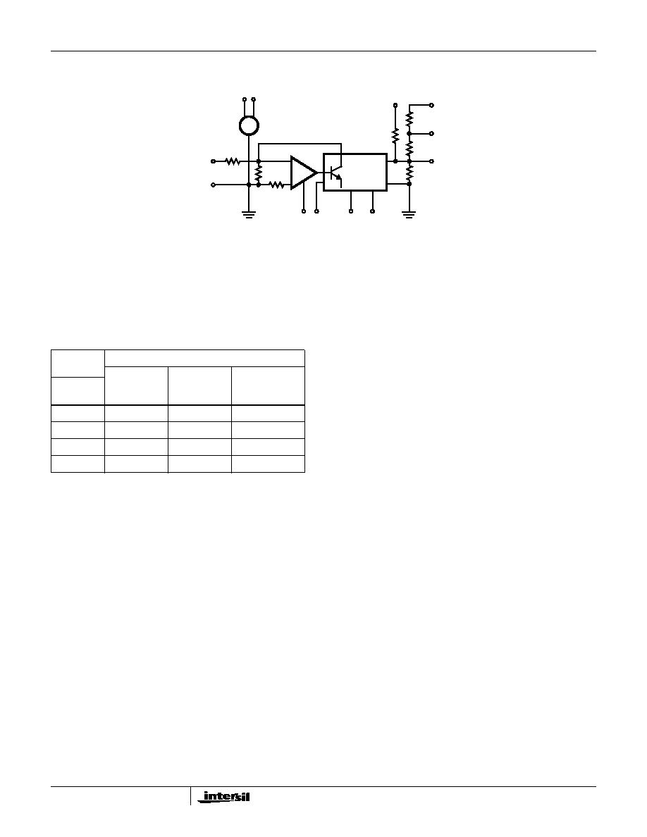
Functional Diagram
Denitions of Specications
Digital Inputs
The HS-565ARH-T accepts digital input codes in binary
format and may be user connected for any one of three
binary codes. Straight binary, Two’s Complement (see note
below), or Offset Binary (see Operating Instructions).
Accuracy
Nonlinearity - Nonlinearity of a D/A converter is an
important measure of its accuracy. It describes the deviation
from an ideal straight line transfer curve drawn between zero
(all bits OFF) and full scale (all bits ON).
Differential Nonlinearity - For a D/A converter, it is the
difference between the actual output voltage change and the
ideal (1 LSB) voltage change for a one bit change in code. A
Differential Nonlinearity of
±1 LSB or less guarantees
monotonicity; i.e., the output always increases and never
decreases for an increasing input.
Settling Time
Settling time is the time required for the output to settle to
within the specied error band for any input code transition.
It is usually specied for a full scale or major carry transition,
settling to within 0.50 LSB of nal value.
Drift
Gain Drift - The change in full scale analog output over the
specied temperature range expressed in parts per million of
full scale range per oC (ppm of FSR/oC). Gain error is
measured with respect to 25oC at high (tH) and low (tL)
temperatures. Gain drift is calculated for both high (tL -
25oC) and low ranges (25oC - tL) by dividing the gain error
by the respective change in temperature. The specication is
the larger of the two representing worst case drift.
Offset Drift - The change in analog output with all bits OFF
over the specied temperature range expressed in parts per
million of full scale range per oC (ppm of FSR/oC). Offset
error is measured with respect to 25oC at high (tH) and low
(tL) temperatures. Offset drift is calculated for both high (tD -
25oC) and low (25oC-tL) ranges by dividing the offset error
by the respective change in temperature. The specication
given is the larger of the two, representing worst case drift.
Power Supply Sensitivity
Power Supply Sensitivity is a measure of the change in
gain and offset of the D/A converter resulting from a
change in -15V or +15V supplies. It is specified under DC
conditions and expressed as parts per million of full scale
range per percent of change in power supply (ppm of
FSR/%).
Compliance
Compliance Voltage is the maximum output voltage range
that can be tolerated and still maintain its specied accuracy.
Compliance Limit implies functional operation only and
makes no claims to accuracy.
Glitch
A glitch on the output of a D/A converter is a transient spike
resulting from unequal internal ON-OFF switching times.
Worst case glitches usually occur at half scale or the major
carry code transition from 011 . . . 1 to 100 . . . 0 or vice
versa. For example, if turn ON is greater than turn OFF for
011 . . . 1 to 100 . . . 0, an intermediate state of 000 . . . 0
exists, such that, the output momentarily glitches toward
zero output. Matched switching times and fast switching will
reduce glitches considerably.
REF OUT VCC
43
+
-
19.95K
REF
10V
6
5
REF
+
-
3.5K
3K
IREF
0.5mA
-VEE
PWR
GND
712
24. . . 13
MSB LSB
(4X IREF
X CODE)
GND
IN
20V
SPAN
10V
SPAN
OUT
IO
DAC
9.95K
BIP.
OFF.
8
5K
2.5K
11
10
9
DIGITAL
INPUT
ANALOG OUTPUT
STRAIGHT
BINARY
OFFSET
BINARY
(NOTE)
TWO’S
COMPLEMENT
MSB . LSB
000 . . . 000
Zero
- fS (Full Scale)
Zero
100 . . . 000
0.50 fS
Zero
- fS
111 . . . 111
+ fS - 1 LSB
Zero - 1 LSB
011 . . . 111
0.50 fS - 1 LSB
Zero - 1 LSB
+ fS - 1 LSB
NOTE: Invert MSB with external inverter to obtain Two’s
Complement Coding.
HS-565ARH-T
相關PDF資料 |
PDF描述 |
|---|---|
| 5962R9675501V9X | PARALLEL, WORD INPUT LOADING, 12-BIT DAC, UUC24 |
| 5962R9675501VXX | PARALLEL, WORD INPUT LOADING, 0.35 us SETTLING TIME, 12-BIT DAC, CDFP24 |
| 5962R9675501VJX | PARALLEL, WORD INPUT LOADING, 0.35 us SETTLING TIME, 12-BIT DAC, CDIP24 |
| 5962R9675501VJX | PARALLEL, WORD INPUT LOADING, 0.35 us SETTLING TIME, 12-BIT DAC, CDIP24 |
| 5962R9675501VXX | PARALLEL, WORD INPUT LOADING, 0.35 us SETTLING TIME, 12-BIT DAC, CQFP24 |
相關代理商/技術參數 |
參數描述 |
|---|---|
| 5962R9679801VCA | 功能描述:校驗器 IC RoHS:否 制造商:STMicroelectronics 產品: 比較器類型: 通道數量: 輸出類型:Push-Pull 電源電壓-最大:5.5 V 電源電壓-最小:1.1 V 補償電壓(最大值):6 mV 電源電流(最大值):1350 nA 響應時間: 最大工作溫度:+ 125 C 安裝風格:SMD/SMT 封裝 / 箱體:SC-70-5 封裝:Reel |
| 5962R9679801VHA | 功能描述:校驗器 IC RoHS:否 制造商:STMicroelectronics 產品: 比較器類型: 通道數量: 輸出類型:Push-Pull 電源電壓-最大:5.5 V 電源電壓-最小:1.1 V 補償電壓(最大值):6 mV 電源電流(最大值):1350 nA 響應時間: 最大工作溫度:+ 125 C 安裝風格:SMD/SMT 封裝 / 箱體:SC-70-5 封裝:Reel |
| 5962R9679801VIA | 功能描述:校驗器 IC RoHS:否 制造商:STMicroelectronics 產品: 比較器類型: 通道數量: 輸出類型:Push-Pull 電源電壓-最大:5.5 V 電源電壓-最小:1.1 V 補償電壓(最大值):6 mV 電源電流(最大值):1350 nA 響應時間: 最大工作溫度:+ 125 C 安裝風格:SMD/SMT 封裝 / 箱體:SC-70-5 封裝:Reel |
| 5962R9679801VXA | 功能描述:校驗器 IC RoHS:否 制造商:STMicroelectronics 產品: 比較器類型: 通道數量: 輸出類型:Push-Pull 電源電壓-最大:5.5 V 電源電壓-最小:1.1 V 補償電壓(最大值):6 mV 電源電流(最大值):1350 nA 響應時間: 最大工作溫度:+ 125 C 安裝風格:SMD/SMT 封裝 / 箱體:SC-70-5 封裝:Reel |
| 5962R9679802VCA | 制造商:Texas Instruments 功能描述:5962R9679802VCA HIGH SPEED DUAL COMPARAT - Rail/Tube |
發布緊急采購,3分鐘左右您將得到回復。