- 您現在的位置:買賣IC網 > PDF目錄56746 > 5962R9675501V9X (INTERSIL CORP) PARALLEL, WORD INPUT LOADING, 12-BIT DAC, UUC24 PDF資料下載
參數資料
| 型號: | 5962R9675501V9X |
| 廠商: | INTERSIL CORP |
| 元件分類: | DAC |
| 英文描述: | PARALLEL, WORD INPUT LOADING, 12-BIT DAC, UUC24 |
| 封裝: | DIE-24 |
| 文件頁數: | 5/7頁 |
| 文件大小: | 125K |
| 代理商: | 5962R9675501V9X |
5
Calibration
Calibration provides the maximum accuracy from a
converter by adjusting its gain and offset errors to zero, For
the HS-565ARH, these adjustments are similar whether the
current output is used, or whether an external op amp is
added to convert this current to a voltage. Refer to Table 7
for the voltage output case, along with Figure 1 or 2.
Calibration is a two step process for each of the ve output
ranges shown in Table 7. First adjust the negative full scale
(zero for unipolar ranges). This is an offset adjust which
translates the output characteristic, i.e. affects each code by
the same amount.
Next adjust positive FS. This is a gain error adjustment, which
rotates the output characteristic about the negative FS value.
For the bipolar ranges, this approach leaves an error at the
zero code, whose maximum values is the same as for
integral nonlinearity error. In general, only two values of
output may be calibrated exactly; all others must tolerate
some error. Choosing the extreme end points (plus and
minus full scale) minimizes this distributed error for all other
codes.
Settling Time
This is a challenging measurement, in which the result
depends on the method chosen, the precision and quality of
test equipment and the operating conguration of the DAC
(test conditions). As a result, the different techniques in use
by converter manufacturers can lead to consistently different
results. An engineer should understand the advantage and
limitations of a given test methods before using the specied
settling time as a basis for design.
The approach used for several years at Intersil calls for a
strobed comparator to sense nal perturbations of the DAC
output waveform. This gives the LSB a reasonable
magnitude (814mV for the HS-565ARH, which provides the
comparator with enough overdrive to establish an accurate
±0.50 LSB window about the nal settled value. Also, the
required test conditions simulate the DACs environment for a
common application - use in a successive approximation
A/D converter. Considerable experience has shown this to
be a reliable and repeatable way to measure settling time.
The usual specication is based on a 10V step, produced by
simultaneously switching all bits from off-to-on (tON) or on-
to-off (tOFF). The slower of the two cases is specied, as
measured from 50% of the digital input transition to the nal
entry within a window of 0.50 LSB about the settled value.
Four measurements characterize a given type of DAC:
(Cases (b) and (c) may be eliminated unless the overshoot
exceeds 0.50 LSB). For example, refer to Figures 3A and 3B
for the measurement of case (d).
Procedure
As shown in Figure 3B, settling time equals tX plus the
comparator delay (tD = 15ns). To measure tX,
Adjust the delay on generator number 2 for a tX of
several microseconds. This assures that the DAC
output has settled to its nal wave.
Switch on the LSB (+5V)
Adjust the VLSB supply for 50% triggering at
COMPARATOR OUT. This is indicated by traces of
equal brightness on the oscilloscope display as shown
in Figure 3B. Note DVM reading.
Switch to LSB to Pulse (P)
Readjust the VLSB supply for 50% triggering as before,
and note DVM reading. One LSB equals one tenth the
difference in the DVM readings noted above.
Adjust the VLSB supply to reduce the DVM reading by
5 LSBs (DVM reads 10X, so this sets the comparator to
sense the nal settled value minus 0.50 LSB).
Comparator output disappears.
Reduce generator number 2 delay until comparator
output reappears, and adjust for “equal brightness”.
Measure tX from scope as shown in Figure 3B. Settling
time equals tX + tD, i.e. tX + 15ns.
(a) tON, to final value +0.50 LSB
(b) tON, to final value -0.50 LSB
(c)
tOFF, to final value +0.50 LSB
(d) OFF, to final value -0.50 LSB
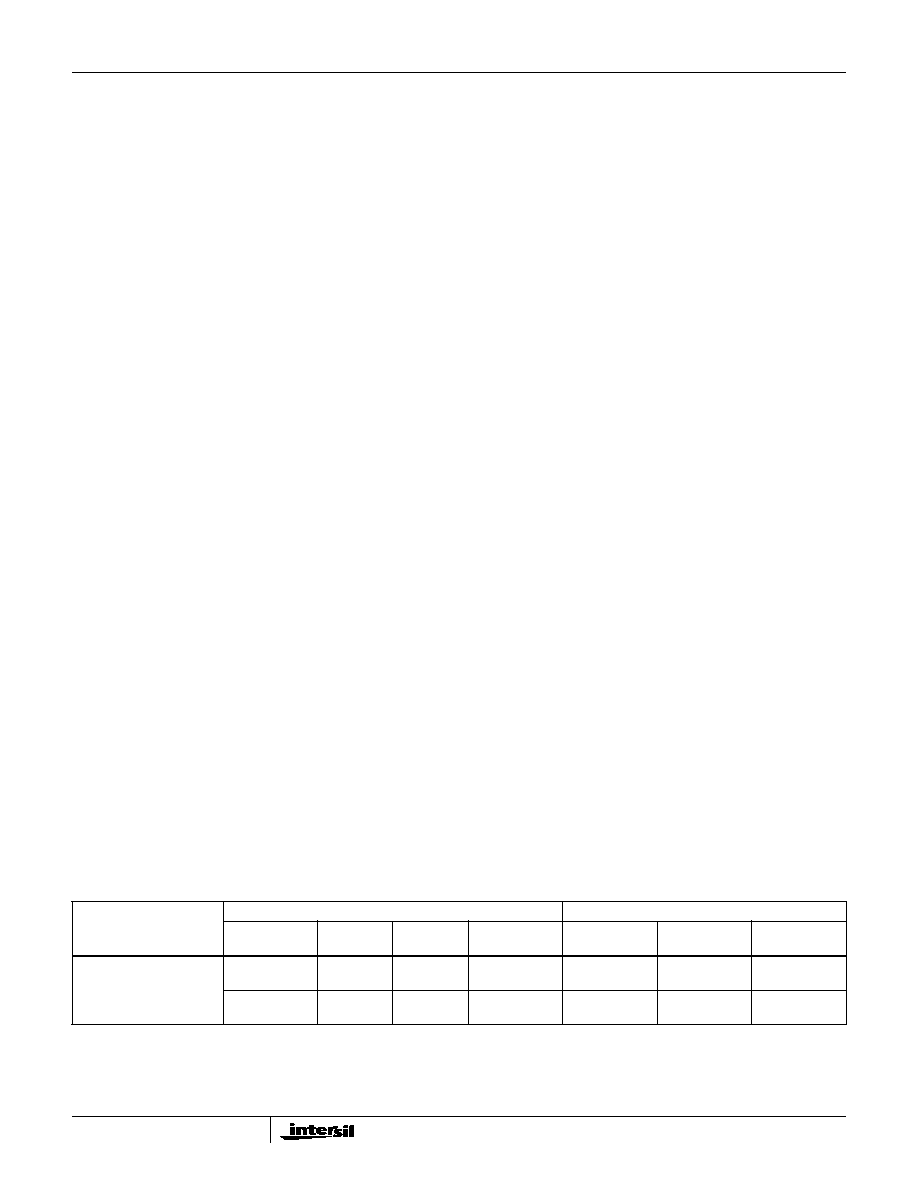
TABLE 1. OPERATING MODES AND CALIBRATION
MODE
CIRCUIT CONNECTIONS
CALIBRATION
OUTPUT
RANGE
PIN 10
TO
PIN 11
TO
RESISTOR
(R)
APPLY
INPUT CODE
ADJUST
TO SET VO
Unipolar (See Figure 1)
0 to +10V
VO
Pin 10
1.43K
All 0’s
All 1’s
R1
R2
0V
+9.99756V
0 to +5V
VO
Pin 9
1.1K
All 0’s
All 1’s
R1
R2
0V
+4.99878V
HS-565ARH
相關PDF資料 |
PDF描述 |
|---|---|
| 5962R9675501VXX | PARALLEL, WORD INPUT LOADING, 0.35 us SETTLING TIME, 12-BIT DAC, CDFP24 |
| 5962R9675501VJX | PARALLEL, WORD INPUT LOADING, 0.35 us SETTLING TIME, 12-BIT DAC, CDIP24 |
| 5962R9675501VJX | PARALLEL, WORD INPUT LOADING, 0.35 us SETTLING TIME, 12-BIT DAC, CDIP24 |
| 5962R9675501VXX | PARALLEL, WORD INPUT LOADING, 0.35 us SETTLING TIME, 12-BIT DAC, CQFP24 |
| 59643-1 | BAND PASS FILTER |
相關代理商/技術參數 |
參數描述 |
|---|---|
| 5962R9679801VCA | 功能描述:校驗器 IC RoHS:否 制造商:STMicroelectronics 產品: 比較器類型: 通道數量: 輸出類型:Push-Pull 電源電壓-最大:5.5 V 電源電壓-最小:1.1 V 補償電壓(最大值):6 mV 電源電流(最大值):1350 nA 響應時間: 最大工作溫度:+ 125 C 安裝風格:SMD/SMT 封裝 / 箱體:SC-70-5 封裝:Reel |
| 5962R9679801VHA | 功能描述:校驗器 IC RoHS:否 制造商:STMicroelectronics 產品: 比較器類型: 通道數量: 輸出類型:Push-Pull 電源電壓-最大:5.5 V 電源電壓-最小:1.1 V 補償電壓(最大值):6 mV 電源電流(最大值):1350 nA 響應時間: 最大工作溫度:+ 125 C 安裝風格:SMD/SMT 封裝 / 箱體:SC-70-5 封裝:Reel |
| 5962R9679801VIA | 功能描述:校驗器 IC RoHS:否 制造商:STMicroelectronics 產品: 比較器類型: 通道數量: 輸出類型:Push-Pull 電源電壓-最大:5.5 V 電源電壓-最小:1.1 V 補償電壓(最大值):6 mV 電源電流(最大值):1350 nA 響應時間: 最大工作溫度:+ 125 C 安裝風格:SMD/SMT 封裝 / 箱體:SC-70-5 封裝:Reel |
| 5962R9679801VXA | 功能描述:校驗器 IC RoHS:否 制造商:STMicroelectronics 產品: 比較器類型: 通道數量: 輸出類型:Push-Pull 電源電壓-最大:5.5 V 電源電壓-最小:1.1 V 補償電壓(最大值):6 mV 電源電流(最大值):1350 nA 響應時間: 最大工作溫度:+ 125 C 安裝風格:SMD/SMT 封裝 / 箱體:SC-70-5 封裝:Reel |
| 5962R9679802VCA | 制造商:Texas Instruments 功能描述:5962R9679802VCA HIGH SPEED DUAL COMPARAT - Rail/Tube |
發布緊急采購,3分鐘左右您將得到回復。