- 您現(xiàn)在的位置:買賣IC網(wǎng) > PDF目錄369224 > 6300 (Linear Technology Corporation) 500mA, 200MHz X DSL LINE DRIVER IN 16-LEAD SSOP PACKAGE PDF資料下載
參數(shù)資料
| 型號: | 6300 |
| 廠商: | Linear Technology Corporation |
| 英文描述: | 500mA, 200MHz X DSL LINE DRIVER IN 16-LEAD SSOP PACKAGE |
| 中文描述: | 500mA的,200MHz的X的DSL線路驅(qū)動器,采用16引線SSOP封裝 |
| 文件頁數(shù): | 7/16頁 |
| 文件大小: | 237K |
| 代理商: | 6300 |
7
LT6300
APPLICATIOU
The LT6300 is a high speed, 200MHz gain bandwidth
product, dual voltage feedback amplifier with high output
current drive capability, 500mA source and sink. The
LT6300 is ideal for use as a line driver in xDSL data
communication applications. The output voltage swing
has been optimized to provide sufficient headroom when
operating from
±
12V power supplies in full-rate ADSL
applications. The LT6300 also allows for an adjustment of
the operating current to minimize power consumption. In
addition, the LT6300 is available in a small footprint
surface mount package to minimize PCB area.
To minimize signal distortion, the LT6300 amplifiers are
decompensated to provide very high open-loop gain at
high frequency. As a result each amplifier is frequency
stable with a closed-loop gain of 10 or more. If a closed-
loop gain of less than 10 is desired, external frequency
compensating components can be used.
W
U
U
Setting the Quiescent Operating Current
Power consumption and dissipation are critical concerns
in multiport xDSL applications. Two pins, Shutdown
(SHDN) and Shutdown Reference (SHDNREF), are pro-
vided to control quiescent power consumption and allow
for the complete shutdown of the driver. The quiescent
current should be set high enough to prevent distortion
induced errors in a particular application, but not so high
that power is wasted in the driver unnecessarily. A good
starting point to evaluate the LT6300 is to set the quiescent
current to 10mA per amplifier.
The internal biasing circuitry is shown in Figure 1. Ground-
ing the SHDNREF pin and directly driving the SHDN pin with
a voltage can control the operating current as seen in the
Typical Performance Characteristics. When the SHDN pin
is less than SHDNREF + 0.4V, the driver is shut down and
consumes typically only 100
μ
A of supply current and the
outputs are in a high impedance state. Part to part varia-
tions, however, will cause inconsistent control of the qui-
escent current if direct voltage drive of the SHDN pin is used.
Using a single external resistor, R
BIAS
, connected in one of
two ways provides a much more predictable control of the
quiescent supply current. Figure 2 illustrates the effect on
supply current per amplifier with R
BIAS
connected be-
tween the SHDN pin and the 12V V
+
supply of the LT6300
and the approximate design equations. Figure 3 illustrates
the same control with R
BIAS
connected between the
SHDNREF pin and ground while the SHDN pin is tied to V
+
.
Either approach is equally effective.
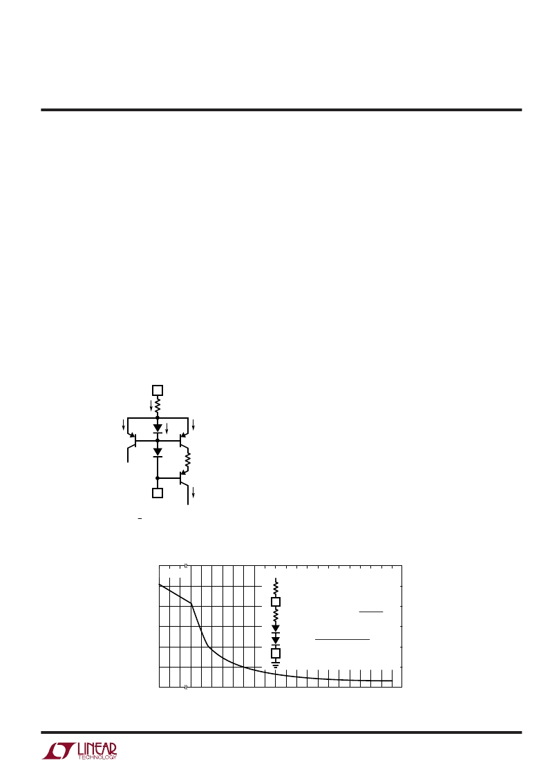
Figure 1. Internal Current Biasing Circuitry
2k
SHDN
SHDNREF
TO
START-UP
CIRCUITRY
1k
6300 F01
I
TO AMPLIFIERS
BIAS CIRCUITRY
2I
I
2I
5I
2
5
I
BIAS
=
I
SUPPLY
PER AMPLIFIER (mA) = 64 I
BIAS
I
SHDN
= I
SHDNREF
R
BIAS
(k
)
0
I
S
10
20
30
5
15
25
10
6300 F02
7
40
70
100
130
160
190
V
S
=
±
12V
V
+
= 12V
R
BIAS
SHDN
SHDNREF
R
BIAS
=
25.6 – 2k
V
+
– 1.2V
I
S
PER AMPLIFIER (mA)
I
S
PER AMPLIFIER
(mA)
25.6
V
+
– 1.2V
R
BIAS
+ 2k
≈
Figure 2. R
BIAS
to V
+
Current Control
相關(guān)PDF資料 |
PDF描述 |
|---|---|
| 6300I | 500mA, 200MHz X DSL LINE DRIVER IN 16-LEAD SSOP PACKAGE |
| 630MMB103JE7TC | METALLIZED POLYESTER FILM CAPACITORS |
| 630MMB103JH7TC | METALLIZED POLYESTER FILM CAPACITORS |
| 630MMB103KE7TC | METALLIZED POLYESTER FILM CAPACITORS |
| 630MMB104JE7TC | METALLIZED POLYESTER FILM CAPACITORS |
相關(guān)代理商/技術(shù)參數(shù) |
參數(shù)描述 |
|---|---|
| 6300 250ML | 制造商:Henkel Corporation / Loctite 功能描述:RETAINER HIGH STRENGTH BOTTL 制造商:Henkel Corporation / Loctite 功能描述:RETAINER HIGH STRENGTH BOTTLE 250ML 制造商:Henkel Corporation / Loctite 功能描述:RETAINER, HIGH STRENGTH, BOTTLE, 250ML |
| 6300 2RS1 | 制造商:UNBRANDED 功能描述:BEARING BALL DOUBLE Z SHIELDED |
| 6300 50ML | 制造商:Henkel Corporation / Loctite 功能描述:RETAINER HIGH STRENGTH BOTTLE 50ML |
| 6300 | 制造商:3M Electronic Products Division 功能描述:Hot melt connector SC connector high r |
| 6300/10 SL001 | 制造商:Alpha Wire Company 功能描述:CBL COMM 10CON 24AWG SLATE 1000' |
發(fā)布緊急采購,3分鐘左右您將得到回復(fù)。