- 您現在的位置:買賣IC網 > PDF目錄369226 > 66012 (Micropac Industries, Inc.) FOUR CHANNEL, HERMETICALLY SEALED, LOW-INPUT CURRENT, 6N140 OPTOCOUPLER PDF資料下載
參數資料
| 型號: | 66012 |
| 廠商: | Micropac Industries, Inc. |
| 英文描述: | FOUR CHANNEL, HERMETICALLY SEALED, LOW-INPUT CURRENT, 6N140 OPTOCOUPLER |
| 中文描述: | 四通道,密封,低輸入電流,6N140光耦合器 |
| 文件頁數: | 2/2頁 |
| 文件大小: | 93K |
| 代理商: | 66012 |
MICROPAC INDUSTRIES, INC.
OPTOELECTRONIC PRODUCTS DIVISION
725 E. Walnut St., Garland, TX 75040
(972) 272-3571
Fax (972) 487-6918
www.micropac.com
E-MAIL: optosales@micropac.com
3 - 28
66012
FOUR CHANNEL, HERMETICALLY SEALED, LOW-INPUT CURRENT, 6N140 OPTOCOUPLER
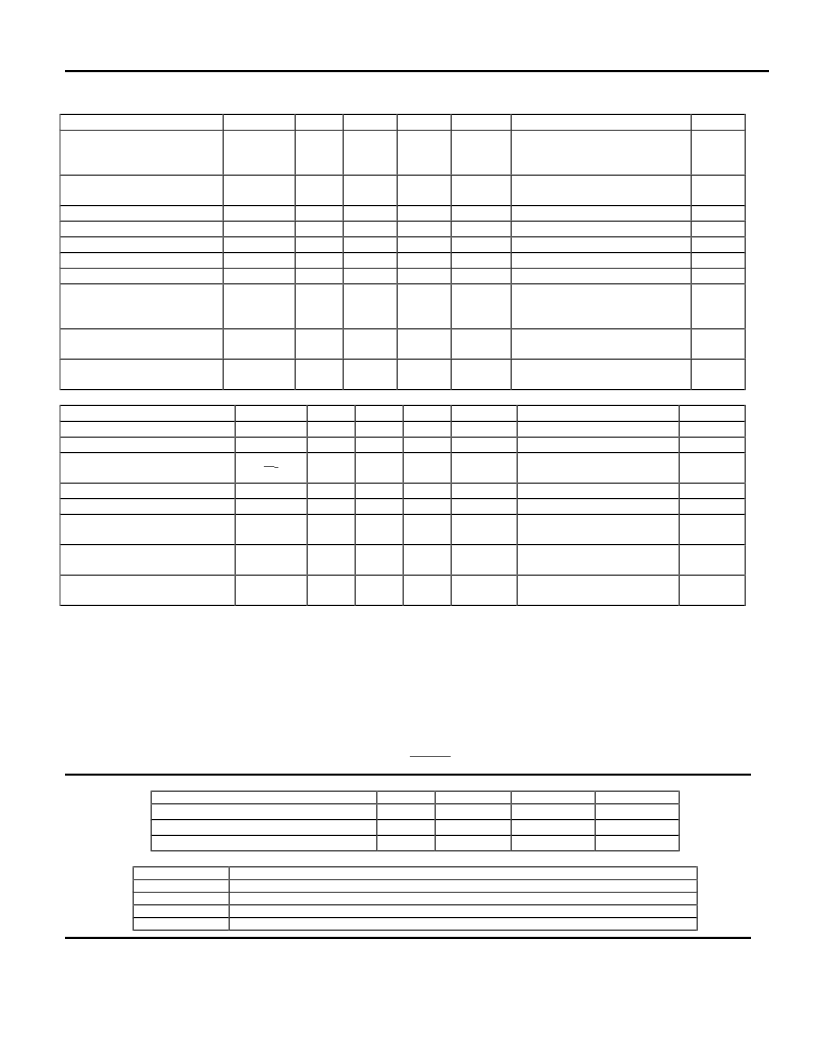
ELECTRICAL CHARACTERISTICS
T
a
= -55
C to 125
C unless otherwise specified.
PARAMETER
Current Transfer Ratio
SYMBOL
CTR
MIN
300
300
200
TYP
1000
750
400
0.1
0.2
.005
.010
2
1.4
MAX
UNITS
%
%
%
V
V
μ
A
μ
A
mA
V
V
μA
TEST CONDITIONS
I
F
= 0.5mA, V
O
= 0.4V, V
CC
= 4.5V
I
F
= 1.6mA, V
O
= 0.4V, V
CC
= 4.5V
I
F
= 5.0mA, V
O
= 0.4V, V
CC
= 4.5V
I
F
= 0.5mA, I
OL
= 1.5mA, V
CC
= 4.5V
I
F
= 5.0mA, I
OL
= 10mA, V
CC
= 4.5V
I
F
= 2
μ
A, V
O
= V
CC
= 18V
I
F1
=I
F2
=I
F3
=I
F4
= 0mA, V
CC
= 18V
I
F1
= I
F2
= I
F3
= I
F4
=1.6mA, V
CC
= 18V
I
F
= 1.6mA
I
R
= 10μA
V
I—0
= 1500Vdc,
Relative Humidity = 45%
t
A
= 25°C, t = 5s
I
F
= 0.5mA, V
CC
= 5.0V, R
L
= 4.7k
I
F
= 5mA, V
CC
= 5.0V, R
L
= 680k
I
F
= 0.5mA, V
CC
= 5.0V, R
L
= 4.7k
I
F
= 5mA, V
CC
= 5.0V, R
L
= 680k
NOTE
1,2
1,2
1,2
1
Logic Low Output Voltage
V
OL
0.4
0.4
250
40
4
1.8
Logic High Output Current
High Level Output Current
Low Level Supply Current
Input Forward Voltage
Input Reverse Breakdown Voltage
Input-Output Insulation Leakage
Current
I
OH
I
CCH
I
CCL
V
F
BV
R
I
I—O
1,3
1
1
4
5
1.0
Propagation Delay Time To High
Output Level
Propagation Delay Time To Low
Output Level
TYPICAL CHARACTERISTICS
T
a
= 25
°
C, V
CC
= 5V Each Channel
PARAMETER
Input Capacitance
Capacitance (Input-Output)
Input Diode Temperature
Coefficient
Resistance (Input-Output)
Resistance (Input-Input)
Input-Input Insulation Leakage
Current
Common Mode Transient immunity
at High Output Level
Common Mode Transient Immunity
at Low Output Level
NOTES:
1.
Each channel.
2.
CURRENT TRANSFER RATIO is defined as the ratio of output collector current, I
O
, to the forward LED input current., I
F
, times 100%.
3.
I
F
= 2
μ
A for channel under test. For all other channels, I
F
= 10mA.
4.
Device considered a two-terminal device. Pins 1-6 and 16 are shorted together and pins 7-14 are shorted together.
5.
Measured between each input pair shorted together.
6.
Measured between adjacent pairs shorted together, i.e. between pins 1 and 2 shorted together and pins 3 and 4 shorted together, etc.
7.
CM
H
is the maximum tolerable common mode transient to assure that the output will remain in a high logic state (ie. V
O
>
@.0V).
8.
CM
L
is the maximum tolerable common mode transient to assure that the output will remain in a low logic state (ie. V
O
<
0.8V).
9.
In applications where dv/dt may exceed 50,000 V/
μ
s (such as static discharge) a series resistor, R
CC
, should be included to protect the detector IC”s
from destructively high surge currents. The recommended value is R
CC
= 1V = k
0.6I
F
(mA)
RECOMMENDED OPERATING CONDITIONS:
PARAMETER
SYMBOL
Input Current, Low Level
Input Current, High Level
Supply Voltage
V
CC
SELECTION GUIDE
PART NUMBER
66012-001
DSCC Dwg 8302401EX Quad Channel Optocoupler
66012-002
Quad Channel optocoupler, commercial, tested over full military temperature range (-55
°
C to +125
°
C)
66012-003
Quad Channel optocoupler, commercial (0
°
to +70
°
C)
66012-004
Quad Channel optocoupler, commercial (-40
°
C to +85
°
C)
t
PLH
5
4
8
2
60
30
100
10
μ
s
μ
s
μ
s
μ
s
t
PHL
SYMBOL
C
IN
C
I-O
v
F
T
A
R
I-0
R
I-I
I
I-I
MIN
TYP
60
1.5
-1.8
MAX
UNITS
pF
pF
mV/
°
C
TEST CONDITIONS
V
F
= 0, f = MHz, t
a
= 25
°
C
f = 1MHz, t
a
= 25
°
C
I
F
= 1.6mA
NOTE
1
1, 5
1
10
12
10
12
0.5
nA
V
I
—O
= 500V, t
a
= 25
°
C
V
I—I
= 500V, t
a
= 25
°
C
Relative Humidity = 45%
V
I—I
= 500V, t = 5s
V
CM
= 50V
P-P
,V
CC
= 5.0V,
R
L
= 1.5k
, I
F
= OmA
V
CM
= 50V
P-P
,V
CC
= 5.0V,
R
L
= 1.5k
, I
F
= 1.6mA
1, 5
6
6
CM
H
500
1000
V/
μ
s
7,9
CM
L
500
1000
V/
μ
s
8,9
MIN
0
0.5
2.0
MAX
2
5
18
UNITS
μ
A
mA
V
I
FL
I
FH
PART DESCRIPTION
相關PDF資料 |
PDF描述 |
|---|---|
| 66012-001 | FOUR CHANNEL, HERMETICALLY SEALED, LOW-INPUT CURRENT, 6N140 OPTOCOUPLER |
| 66012-002 | FOUR CHANNEL, HERMETICALLY SEALED, LOW-INPUT CURRENT, 6N140 OPTOCOUPLER |
| 66012-003 | FOUR CHANNEL, HERMETICALLY SEALED, LOW-INPUT CURRENT, 6N140 OPTOCOUPLER |
| 66012-004 | FOUR CHANNEL, HERMETICALLY SEALED, LOW-INPUT CURRENT, 6N140 OPTOCOUPLER |
| 66013 | DUAL CHANNEL, HERMETICALLY SEALED, HIGH-SPEED 6N134 OPTOCOUPLER |
相關代理商/技術參數 |
參數描述 |
|---|---|
| 6-601-2 | 制造商:Eaton Corporation 功能描述:CONTACT KIT, CITATION, SIZE 6, SERIES C1, 2 POLE |
| 6601-20-01 | 制造商:SPC Multicomp 功能描述:IC SOCKET PLCC SMD 20WAY TUBE/39 |
| 66012-001 | 制造商:MII 制造商全稱:MII 功能描述:FOUR CHANNEL, HERMETICALLY SEALED, LOW-INPUT CURRENT, 6N140 OPTOCOUPLER |
| 6601-20-01-18 | 制造商:SPC Multicomp 功能描述:IC SOCKET PLCC SMD 20WAY |
| 6601-20-01-18-F6 | 制造商:SPC Multicomp 功能描述:SOCKET IC PLCC SMD 20WAY |
發布緊急采購,3分鐘左右您將得到回復。