- 您現在的位置:買賣IC網 > PDF目錄369227 > 66079-005H (MICROPAC INDUSTRIES INC) OPTICALLY COUPLED DIGITAL FILTER PDF資料下載
參數資料
| 型號: | 66079-005H |
| 廠商: | MICROPAC INDUSTRIES INC |
| 元件分類: | 光電耦合器 |
| 英文描述: | OPTICALLY COUPLED DIGITAL FILTER |
| 中文描述: | 1 CHANNEL LOGIC OUTPUT OPTOCOUPLER, 10 Mbps |
| 封裝: | HERMETIC SEALED PACKAGE-6 |
| 文件頁數: | 1/2頁 |
| 文件大小: | 92K |
| 代理商: | 66079-005H |
MICROPAC INDUSTRIES, INC.
OPTOELECTRONIC PRODUCTS DIVISION
725 E. Walnut St., Garland, TX 75040
(972) 272-3571
Fax (972) 487-6918
www.micropac.com
E-MAIL: optosales@micropac.com
3 - 38
66079
OPTICALLY COUPLED DIGITAL FILTER
Mii
OPTOELECTRONIC PRODUCTS
DIVISION
Features:
DSCC Approved 916761HXX
10 MBd typical
Meets Tempest EMI/RFI emanation criteria
TTL compatible input and output
RFI Rejection 80dB to 1GHz
Faraday shield to provide high common mode
rejection
Applications:
Military and space
Secure communication systems
Isolated receiver input
Microprocessor system interface
Digital isolation for A/D, D/A converters
DESCRIPTION
The
66079
Optically Coupled Digital Filter consists of an LED optically coupled to a high speed, high gain inverting detector
gate. Maximum isolation can be achieved while providing a TTL output capable of switching with propagation delays of 55nS
typical. The 66079 is a hermetically sealed package which is threaded in order to provide convenient bulkhead mounting and
is available in standard and screened versions or tested to customer specifications. The 66079-001 is a hermetically sealed
package which can be soldered or press-fit mounted and is also available in standard and MIL-PRF-38534 screened versions
or tested to customer specifications.
ABSOLUTE MAXIMUM RATINGS
Storage Temperature.............................................................................................................................................-65°C to +150°C
Operating Free-Air Temperature Range...............................................................................................................-55°C to +125°C
Lead Solder Temperature...........................................................................................260
°
C for 10s (1.6mm below seating plane)
Peak Forward Input Current ..........................................................................................................................40mA (1ms duration)
Forward Input Current Continuous ........................................................................................................................................ 20mA
Supply voltage - V
CC
..................................................................................................................................7V(1 minute maximum)
Output Current - I
O
................................................................................................................................................................. 25mA
Output Power Dissipation...................................................................................................................................................... 40mW
Output Voltage - V
O
.....................................................................................................................................................................7V
Total Power Dissipation ...................................................................................................................................................... 175mW
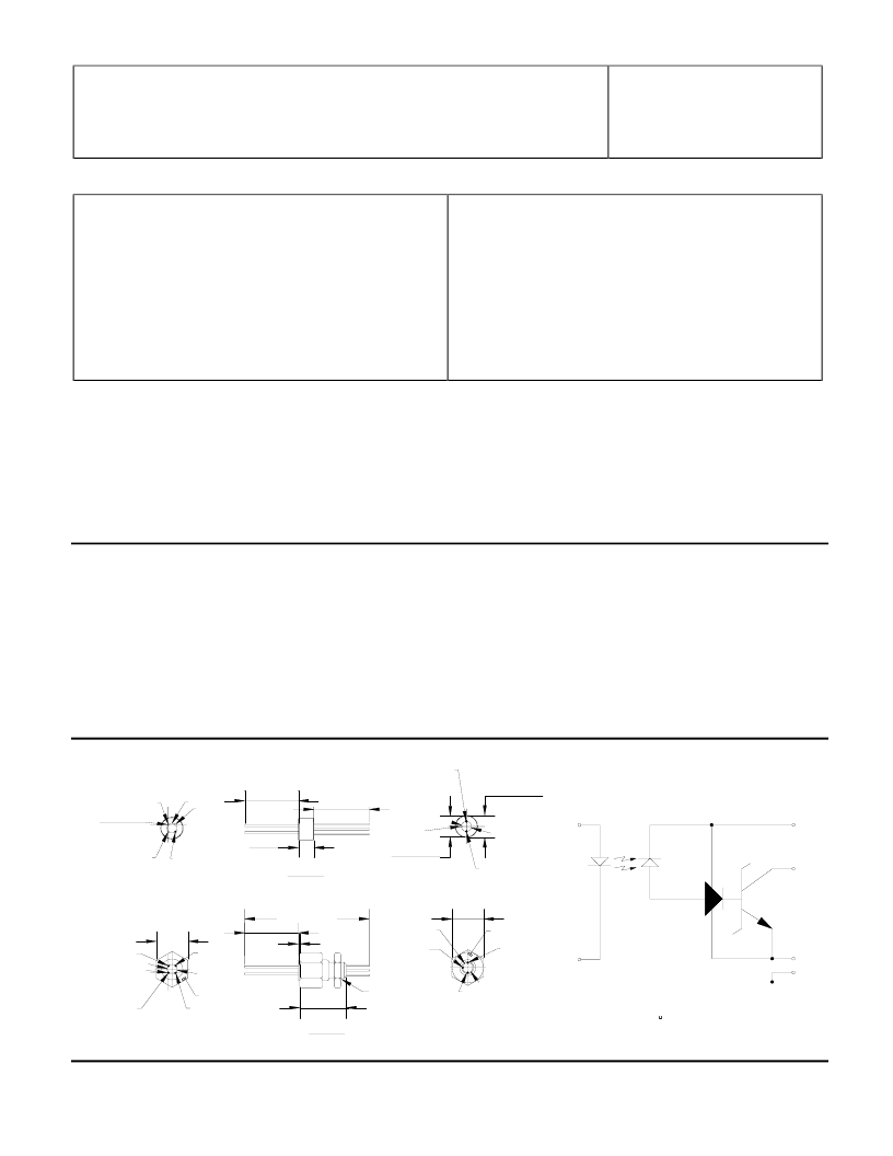
Package Dimensions
Schematic Diagram
OUT
V
.100 ± .005
Vcc
GROUND
NC
0.019 [0.483]
0.221 [5.613]
0.209 [5.309]
N.C.
ANODE
CATHODE
0.100 ± .005 [2.540]
66079-001
0.019 [0.483]
GROUND
N.C.
RED POINT
V OUT
Vcc
0.100 ±.005
0.100 ±.005
RED POINT
N.C.
CATHODE
ANODE
1.230 [31.231]
0.01MAX
THREADS ARE .250± .010
40 ± 0.1 TURNS PER INCH
66079-000
ALL DIMENSIONS ARE IN INCHES [MILLIMETERS]
ALL DIMENSIONS ARE IN INCHES [MILLIMETERS]
Vcc AND GROUND.
CONNECTED BETWEEN
CAPACITOR MUST BE
A.01 TO 0.1
NOTE:
F BYPASS
GND
CASE
OUT
VCC
A
K
0.532 [13.521]
0.562 [14.283]
0.500 [12.691]
0.560 [14.215]
0.137 [3.480]
0.167 [4.242]
0.312 ±.005
[7.935]
0.500 [12.691]
0.453 [11.506]
0.312 ±.005
[7.935]
相關PDF資料 |
PDF描述 |
|---|---|
| 66079 | OPTICALLY COUPLED DIGITAL FILTER |
| 6609018-2 | EMI/RFI Filters and Accessories |
| 6609018-6 | EMI/RFI Filters and Accessories |
| 6609018-8 | EMI/RFI Filters and Accessories |
| 6609033-8 | EMI/RFI Filters and Accessories |
相關代理商/技術參數 |
參數描述 |
|---|---|
| 6608 | 制造商:AEMC Instruments 功能描述:PHASE ROTATION METER, 15-400HZ; Frequency Measuring Range:15Hz to 400Hz; Operating Temperature Min:0C; Operating Temperature Max:40C; External Height:130mm; External Width:69mm; External Depth:32mm; Weight:130g 制造商:AEMC Instruments 功能描述:PHASE ROTATION METER, 15-400HZ; Frequency Measuring Range:15Hz to 400Hz; Operating Temperature Min:0C; Operating Temperature Max:40C; External Height:130mm; External Width:69mm; External Depth:32mm; Weight:130g ;RoHS Compliant: NA |
| 660-8 | 制造商:TUSKERS 功能描述:EXEC BLK S/MIDSOL SHOE 8 |
| 6608 CL05 | 制造商:Aavid Thermalloy 功能描述:- Bulk |
| 66080 | 功能描述:MAT RUBBER DISS 2X40'.06" DK GRY RoHS:否 類別:靜電控制,ESD,無塵室產品 >> 接地墊 系列:Statfree T2™ 標準包裝:1 系列:Statfree B2™ 墊子類型:桌子,工作臺卷筒 形狀:矩形 長度:50' (15.24m) 寬:2'(0.61m) 厚度:0.06" (1.52mm) 顏色:深藍色 材質:橡膠 特點:導電,靜電耗散 包括:- |
| 66-080000-017 | 制造商:Chenbro Micom Usa, Inc. 功能描述:CHENBRO 66-080000-017 - Bulk |
發布緊急采購,3分鐘左右您將得到回復。