- 您現在的位置:買賣IC網 > PDF目錄222756 > 66083-201 (MICROPAC INDUSTRIES INC) 1 CHANNEL TRANSISTOR OUTPUT OPTOCOUPLER PDF資料下載
參數資料
| 型號: | 66083-201 |
| 廠商: | MICROPAC INDUSTRIES INC |
| 元件分類: | 光電耦合器 |
| 英文描述: | 1 CHANNEL TRANSISTOR OUTPUT OPTOCOUPLER |
| 封裝: | HERMETIC SEALED, LCC-4 |
| 文件頁數: | 1/2頁 |
| 文件大小: | 84K |
| 代理商: | 66083-201 |
MICROPAC INDUSTRIES, INC. OPTOELECTRONIC PRODUCTS DIVISION 725 E. Walnut St., Garland, TX 75040 (972) 272-3571 Fax (972) 487-6918
www.micropac.com
E-MAIL: optosales@micropac.com
3 - 10
66083
SINGLE CHANNEL OPTOCOUPLERS
Mii
OPTOELECTRONIC PRODUCTS
DIVISION
REVISION A 12/29/00
Features:
Collector is electrically isolated from the case.
Overall current gain...1.5 typical (-X03)
Rugged package
High gain, high voltage transistor
+1kV electrical isolation
Applications:
Eliminate ground loops
Level shifting
Line receiver
Switching power supplies
Motor control
DESCRIPTION
The 66083 series optocoupler consist of a Gallium Aluminum Arsenide (GaAlAs) infrared LED and a high gain N-P-N silicon
phototransistor packaged in a hermetically sealed LCC case. The 66083 can be tested to customer specifications, as well as
to MIL-PRF-19500 JAN, JANS, JANTX, and JANTXV quality levels.
*ABSOLUTE MAXIMUM RATINGS
Input to Output Voltage.............................................................................................................................................................±1kV
Emitter-Collector Voltage..............................................................................................................................................................5V
Collector-Emitter Voltage............................................................................................................................................................35V
Reverse Input Voltage .................................................................................................................................................................2V
Input Diode Continuous Forward Current at (or below) 65°C Free-Air Temperature (see note 1) ....................................... 40mA
Peak Forward Input Current (Value applies for tw < 1s, PRR < 300 pps) .................................................................................1A
Continuous Collector Current ................................................................................................................................................. 50mA
Continuous Transistor Power Dissipation at (or below) 25°C Free-Air Temperature (see Note 2) ................................... 300mW
Storage Temperature............................................................................................................................................. -65°C to +125°C
Operating Free-Air Temperature Range ............................................................................................................... -55°C to +125°C
Lead Solder Temperature (1/16” (1.6mm) from case for 10 seconds) ..................................................................................240°C
Notes:
1. Derate linearly to 125°C free-air temperature at the rate of 0.67 mA/°C above 65°C.
2. Derate linearly to 125°C free-air temperature at the rate of 5 mW/°C.
* JEDEC registered data
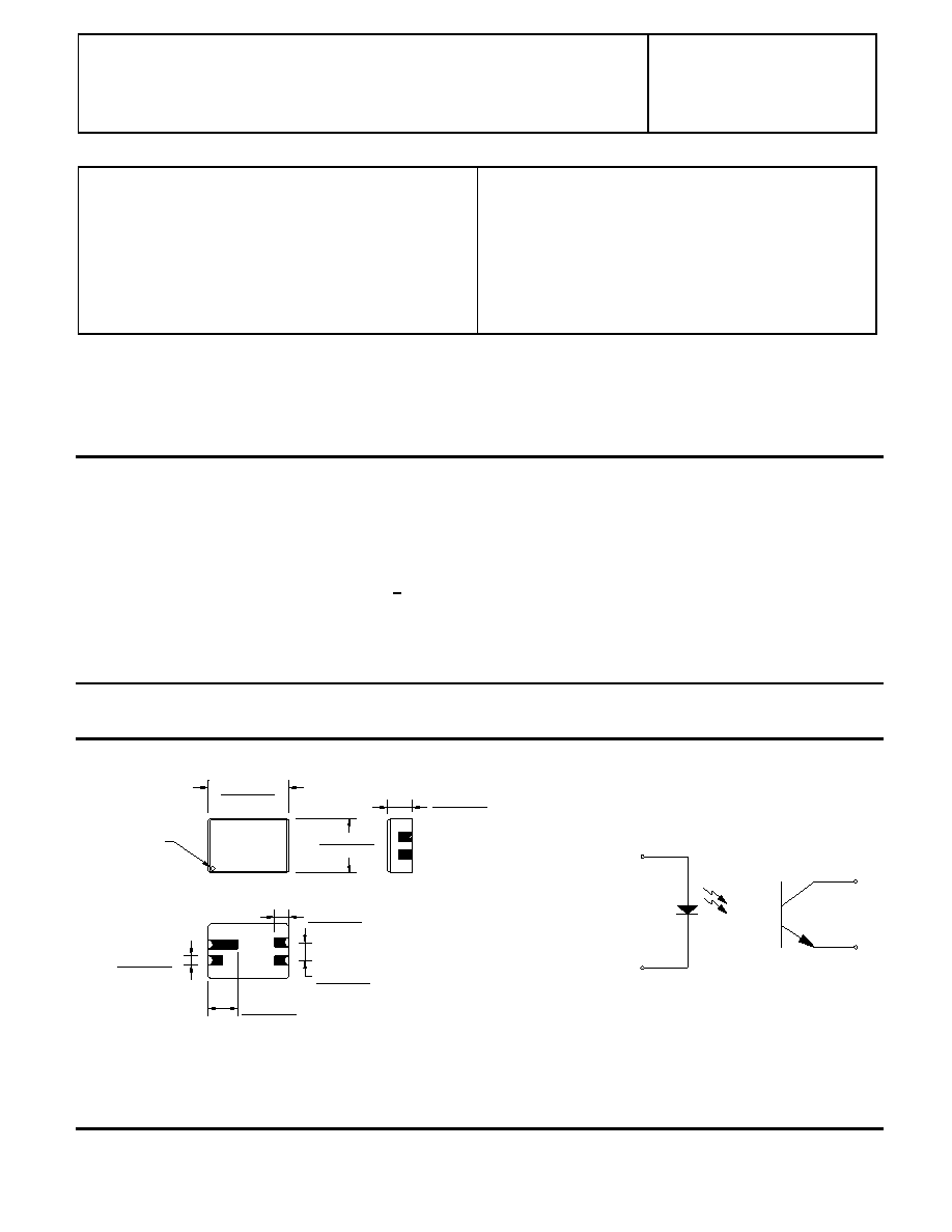
Package Dimensions
Schematic Diagram
K
A
C
E
1
3
2
4
ALLDIMENSIONSAREININCHES[MILLIMETERS]
0.088[2.24]
1
4
0.048[1.22]
2
3
0.225[5.72]
IDENTIFIER
PIN1
0.028[0.17]
0.055[1.40]
0.215[5.46]
0.145[3.68]
0.155[1.40]
0.061[1.55]
0.075[1.91]
0.032[0.81]
3PL
0.045[1.14]
0.072[1.83]
0.022[0.56]
相關PDF資料 |
PDF描述 |
|---|---|
| 66143-003 | 4 CHANNEL TRANSISTOR OUTPUT OPTOCOUPLER |
| 66177-101 | 1 CHANNEL LOGIC OUTPUT OPTOCOUPLER |
| 66177-003 | 1 CHANNEL LOGIC OUTPUT OPTOCOUPLER |
| 66192-002 | 1 CHANNEL LOGIC OUTPUT OPTOCOUPLER |
| 66225-101 | 1 CHANNEL LINEAR OUTPUT OPTOCOUPLER |
相關代理商/技術參數 |
參數描述 |
|---|---|
| 66084-1 | 制造商:TE Connectivity 功能描述:CONN CONT 1 POS - Bulk 制造商:TE Connectivity 功能描述:Contact SKT Crimp ST Cable Mount |
| 66084-2 | 功能描述:標準卡緣連接器 TERM DUMMY TIN .156 RoHS:否 制造商:3M Electronic Solutions Division 系列:SPD08 產品類型:Contacts 位置/觸點數量:60 安裝角:Straight 電路板厚度: 安裝風格:SMD/SMT 節距:8 mm 外殼材料:Liquid Crystal Polymer (LCP) 觸點材料:Copper Alloy 觸點電鍍:Gold |
| 66084-3 | 功能描述:標準卡緣連接器 CONT AMP LEAF L/P 30 RoHS:否 制造商:3M Electronic Solutions Division 系列:SPD08 產品類型:Contacts 位置/觸點數量:60 安裝角:Straight 電路板厚度: 安裝風格:SMD/SMT 節距:8 mm 外殼材料:Liquid Crystal Polymer (LCP) 觸點材料:Copper Alloy 觸點電鍍:Gold |
| 66085 | 功能描述:RUBBER DISS GREY .060 36X40' RoHS:否 類別:靜電控制,ESD,無塵室產品 >> 接地墊 系列:Statfree T2™ 標準包裝:1 系列:Statfree B2™ 墊子類型:桌子,工作臺卷筒 形狀:矩形 長度:50' (15.24m) 寬:2'(0.61m) 厚度:0.06" (1.52mm) 顏色:深藍色 材質:橡膠 特點:導電,靜電耗散 包括:- |
| 66086 | 功能描述:MAT RUBBER DRK BLUE 36"X40' RoHS:是 類別:靜電控制,ESD,無塵室產品 >> 接地墊 系列:Statfree T2™ 標準包裝:1 系列:Statfree B2™ 墊子類型:桌子,工作臺卷筒 形狀:矩形 長度:50' (15.24m) 寬:2'(0.61m) 厚度:0.06" (1.52mm) 顏色:深藍色 材質:橡膠 特點:導電,靜電耗散 包括:- |
發布緊急采購,3分鐘左右您將得到回復。