- 您現在的位置:買賣IC網 > PDF目錄369228 > 66168 (Micropac Industries, Inc.) PROTON RADIATION TOLERANT OPTOCOUPLER (Pin-for-Pin Replacement for 4N49) PDF資料下載
參數資料
| 型號: | 66168 |
| 廠商: | Micropac Industries, Inc. |
| 英文描述: | PROTON RADIATION TOLERANT OPTOCOUPLER (Pin-for-Pin Replacement for 4N49) |
| 中文描述: | 質子輻射容錯光耦合器(引腳對引腳換4N49) |
| 文件頁數: | 1/2頁 |
| 文件大小: | 86K |
| 代理商: | 66168 |
MICROPAC INDUSTRIES, INC.
OPTOELECTRONIC PRODUCTS DIVISION
725 E. Walnut St., Garland, TX 75040
(972)272-3571
Fax (972)487-6918
www.micropac.com
E-MAIL: OPTOSALES @ MICROPAC.COM
3 - 16
66168
PROTON RADIATION TOLERANT OPTOCOUPLER
(Pin-for-Pin Replacement for 4N49)
Mii
OPTOELECTRONIC PRODUCTS
DIVISION
Rev. A 4/25/00
Features:
High Reliability
Base lead provided for conventional transistor
biasing
Rugged package
Stability over wide temperature
+1000V electrical isolation
DESCRIPTION
The
66168
is a modified 4N49 (LED) designed to be more tolerant to proton radiation. The 66168 optocoupler is packaged
in a hermetically sealed TO-5. This device can be supplied to customer specifications as well as tested in accordance with
MIL-PRF-19500/548 (4N49) to JAN, JANTX, JANTXV and JANS levels.
ABSOLUTE MAXIMUM RATINGS
Input to Output Voltage.........................................................................................................................................................+1kV
Emitter-Base Voltage................................................................................................................................................................7V
Collector-Emitter Voltage (Value applies to emitter-base open-circuited & the input-diode equal to zero)..........................40V
Collector-Base Voltage...........................................................................................................................................................45V
Reverse Input Voltage .............................................................................................................................................................2V
Input Diode Continuous Forward Current at (or below) 65°C Free-Air Temperature (see note 1)....................................40mA
Peak Forward Input Current (Value applies for tw
<
1
μ
s, PRR
<
300 pps) .............................................................................1A
Continuous Collector Current..............................................................................................................................................50mA
Continuous Transistor Power Dissipation at (or below) 25°C Free-Air Temperature (see Note 2) ................................300mW
Storage Temperature..........................................................................................................................................-65°C to +125°C
Operating Free-Air Temperature Range............................................................................................................-55°C to +100°C
Lead Solder Temperature (10 seconds max.) ...................................................................................................................240°C
Notes:
1. Derate linearly to 125°C free-air temperature at the rate of 0.67 mA/°C above 65°C.
2. Derate linearly to 125°C free-air temperature at the rate of 3 mW/°C.
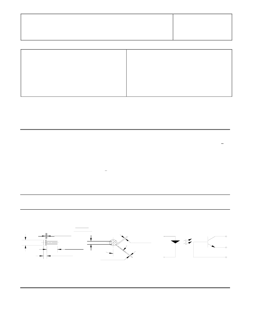
Package Dimensions
Schematic Diagram
Applications:
Eliminate ground loops
Level shifting
Line receiver
Switching power supplies
Motor control
N O TE : A LL LIN E AR D IM EN S IO N S AR E IN IN C H ES (M ILLIM ETER S )
6 LEA D S
0.016 [0.41]
0.019 [0.48]
1
2
3
5
6
7
0.335 [8.51]
0.305 [7.75]
M IN .
0.040 [1.02]
M AX.
0.500 [12.70]
0.155 [3.94]
0.185 [4.70]
0.045 [1.14]
0.029 [0.73]
0.034 [0.864]
0.028 [0.711]
45°
3
5
E
B
K
7
2
1
C
A
0.022 [5.08]
相關PDF資料 |
PDF描述 |
|---|---|
| 66168-300 | PROTON RADIATION TOLERANT OPTOCOUPLER (Pin-for-Pin Replacement for 4N49) |
| 66168-001 | PREMIUM RS232 DATA CBL DB25 MALE - DB25 FEMALE |
| 66168-101 | PREMIUM RS232 DATA CBL DB25 MALE - DB25 MALE |
| 66168-103 | TELCO 50-PAIR PVC 50 FT 4 CNNCTRS MALE/MALE |
| 66168-105 | MAGNETIC FLEXIBLE NECK LIGHT |
相關代理商/技術參數 |
參數描述 |
|---|---|
| 66168-001 | 制造商:Micropac Industries Inc 功能描述:Optocoupler DC-IN 1-CH Transistor With Base DC-OUT 6-Pin TO-5 |
| 66168-009 | 制造商:FCI 功能描述:SUB D RECP PLASTIC 9 POS |
| 66168-015 | 制造商:FCI 功能描述:SUB D RECP PLASTIC 15 POS |
| 66168-025 | 制造商:FCI 功能描述:SUB D RECP PLASTIC 25 POS |
| 66168-101 | 制造商:MII 制造商全稱:MII 功能描述:PROTON RADIATION TOLERANT OPTOCOUPLER (Pin-for-Pin Replacement for 4N49) |
發布緊急采購,3分鐘左右您將得到回復。