- 您現在的位置:買賣IC網 > PDF目錄294088 > 70V34S20PFGI (INTEGRATED DEVICE TECHNOLOGY INC) 4K X 18 DUAL-PORT SRAM, 20 ns, PQFP100 PDF資料下載
參數資料
| 型號: | 70V34S20PFGI |
| 廠商: | INTEGRATED DEVICE TECHNOLOGY INC |
| 元件分類: | SRAM |
| 英文描述: | 4K X 18 DUAL-PORT SRAM, 20 ns, PQFP100 |
| 封裝: | 14 X 14 MM, 1.40 MM HEIGHT, GREEN, PLASTIC, TQFP-100 |
| 文件頁數: | 8/25頁 |
| 文件大小: | 211K |
| 代理商: | 70V34S20PFGI |
6.42
IDT70V35/34S/L
(IDT70V25/24S/L)
High-Speed 3.3V 8/4K x 18 (8/4K x 16) Dual-Port Static RAM
Industrial and Commercial Temperature Ranges
16
5624 drw 13
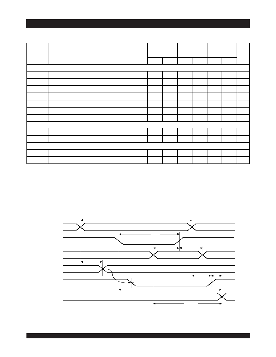
tAPS
ADDR"A"
tWC
DATAOUT "B"
MATCH
tWP
R/
W"A"
DATAIN "A"
ADDR"B"
tDH
VALID
(1)
MATCH
BUSY"B"
tBDA
VALID
tBDD
tDDD(3)
tWDD
tBAA
tDW
Timing Waveform of Write Port-to-Port Read and BUSY(2,4,5) (M/S = VIH)
NOTES:
1. To ensure that the earlier of the two ports wins. tAPS is ignored for M/
S = VIL (slave).
2.
CEL = CER = VIL.
3.
OE = VIL for the reading port.
4. If M/
S = VIL (slave), BUSY is an input. Then for this example BUSY“A” = VIH and BUSY“B” input is shown above.
5. All timing is the same for both left and right ports. Port “A” may be either the left or right port. Port “B ” is the port opposite from port “A”.
AC Electrical Characteristics Over the Operating
Temperature and Supply Voltage Range for 70V35/34(6)
NOTES:
1. Port-to-port delay through SRAM cells from writing port to reading port, refer to "TIMING WAVEFORM OF WRITE PORT-TO-PORT READ AND
BUSY (M/S = VIH)".
2. To ensure that the earlier of the two ports wins.
3. tBDD is a calculated parameter and is the greater of 0, tWDD – tWP (actual) or tDDD – tDW (actual).
4. To ensure that the write cycle is inhibited during contention.
5. To ensure that a write cycle is completed after contention.
6. 'X' in part number indicates power rating (S or L).
70V35/34X15
Com'l Ony
70V35/34X20
Com'l
& Ind
70V35/34X25
Com'l Only
Symbol
Parameter
Min.Max.Min.Max.
Min.
Max.
Unit
BUSY TIMING (M/S = VIH)
tBAA
BUSY Access Time from Address Match
____
15
____
20
____
20
ns
tBDA
BUSY Disable Time from Address Not Matched
____
15
____
20
____
20
ns
tBAC
BUSY Access Time from Chip Enable LOW
____
15
____
20
____
20
ns
tBDC
BUSY Dis able Time from Chip Enable HIGH
____
15
____
17
____
17
ns
tAPS
Arbitration Priority Set-up Time
(2)
5
____
5
____
5
____
ns
tBDD
BUSY Disable to Valid Data(3)
____
18
____
30
____
30
ns
tWH
Write Hold After
BUSY(5)
12
____
15
____
17
____
ns
BUSY TIMING (M/S = VIL)
tWB
BUSY Input to Write(4)
0
____
0
____
0
____
ns
tWH
Write Hold After
BUSY(5)
12
____
15
____
17
____
ns
PORT-TO-PORT DELAY TIMING
tWDD
Write Pulse to Data Delay
(1)
____
30
____
45
____
50
ns
tDDD
Write Data Valid to Read Data Delay
(1)
____
25
____
35
____
35
ns
5624 tbl 13
相關PDF資料 |
PDF描述 |
|---|---|
| 710-405J12 | STEEL, CIRCULAR ADAPTER |
| 710-405J16 | STEEL, CIRCULAR ADAPTER |
| 710-405J24 | STEEL, CIRCULAR ADAPTER |
| 710-405J32 | STEEL, CIRCULAR ADAPTER |
| 710-405J40 | STEEL, CIRCULAR ADAPTER |
相關代理商/技術參數 |
參數描述 |
|---|---|
| 70V34S25PF | 功能描述:靜態隨機存取存儲器 RoHS:否 制造商:Cypress Semiconductor 存儲容量:16 Mbit 組織:1 M x 16 訪問時間:55 ns 電源電壓-最大:3.6 V 電源電壓-最小:2.2 V 最大工作電流:22 uA 最大工作溫度:+ 85 C 最小工作溫度:- 40 C 安裝風格:SMD/SMT 封裝 / 箱體:TSOP-48 封裝:Tray |
| 70V34S25PF8 | 功能描述:靜態隨機存取存儲器 RoHS:否 制造商:Cypress Semiconductor 存儲容量:16 Mbit 組織:1 M x 16 訪問時間:55 ns 電源電壓-最大:3.6 V 電源電壓-最小:2.2 V 最大工作電流:22 uA 最大工作溫度:+ 85 C 最小工作溫度:- 40 C 安裝風格:SMD/SMT 封裝 / 箱體:TSOP-48 封裝:Tray |
| 70V3569S4BC | 功能描述:靜態隨機存取存儲器 RoHS:否 制造商:Cypress Semiconductor 存儲容量:16 Mbit 組織:1 M x 16 訪問時間:55 ns 電源電壓-最大:3.6 V 電源電壓-最小:2.2 V 最大工作電流:22 uA 最大工作溫度:+ 85 C 最小工作溫度:- 40 C 安裝風格:SMD/SMT 封裝 / 箱體:TSOP-48 封裝:Tray |
| 70V3569S4BC8 | 制造商:Integrated Device Technology Inc 功能描述:SRAM Chip Sync Dual 3.3V 576K-Bit 16K x 36 4.2ns 256-Pin CABGA T/R 制造商:Integrated Device Technology Inc 功能描述:SRAM SYNC DUAL 3.3V 576KBIT 16KX36 4.2NS 256BGA - Tape and Reel |
| 70V3569S4BF | 功能描述:靜態隨機存取存儲器 RoHS:否 制造商:Cypress Semiconductor 存儲容量:16 Mbit 組織:1 M x 16 訪問時間:55 ns 電源電壓-最大:3.6 V 電源電壓-最小:2.2 V 最大工作電流:22 uA 最大工作溫度:+ 85 C 最小工作溫度:- 40 C 安裝風格:SMD/SMT 封裝 / 箱體:TSOP-48 封裝:Tray |
發布緊急采購,3分鐘左右您將得到回復。