- 您現在的位置:買賣IC網 > PDF目錄369269 > 73007 (Vishay Intertechnology,Inc.) DC-DC Converter, 2Watt, Input VDC: 24, Output VDC: 7.2/-7.2, Max Output Current(A): ??0.139, Package: SIP7, Isolation(VDC): 1000, Operating Temp. -40??C to +85??C, Low Ripple & Noise, High Efficiency up to 85%, Low Profile Plastic Case, Single, Dual & Dual Separated Outputs PDF資料下載
參數資料
| 型號: | 73007 |
| 廠商: | Vishay Intertechnology,Inc. |
| 元件分類: | DC/DC變換器 |
| 英文描述: | DC-DC Converter, 2Watt, Input VDC: 24, Output VDC: 7.2/-7.2, Max Output Current(A): ??0.139, Package: SIP7, Isolation(VDC): 1000, Operating Temp. -40??C to +85??C, Low Ripple & Noise, High Efficiency up to 85%, Low Profile Plastic Case, Single, Dual & Dual Separated Outputs |
| 中文描述: | 9線端接SCSI總線 |
| 文件頁數: | 1/10頁 |
| 文件大小: | 86K |
| 代理商: | 73007 |
SiP5630
Vishay Siliconix
New Product
Document Number: 73007
S-41263—Rev. A, 05-Ju1-04
www.vishay.com
1
9-Line SCSI Bus Terminators
FEATURES
Auto Selection of S/E or LVD SCSI Termination
2.7-V to 5.25-V TERMPWR Range
Meets SCSI-1, SCSI-2, SPI-2 (ULTRA-2), SPI-3
(ULTRA-160) and SPI-4 (ULTRA-320) Standards
Differential Failsafe Bias
Thermal Package
On-Chip Thermal Shutdown Circuit
Master/Slave Input
Active Negation
Hot Swap Compatible
Pin Compatible with UCC5630 and UCC5670
Lead (Pb)-Free QSOP-36 Package
APPLICATIONS
Disk Array (RAID)
Storage Area Networks (SAN)
Network Attached Storage (NAS)
SCSI Cable
Server and Workstation
Industrial Computers
High-End Personal Computers
DESCRIPTION
The SiP5630 provides active bus termination suitable for all
SCSI bus operational modes from SCSI-1 through SPI-4
(Ultra 320). The termination includes impedance matching of
the SCSI bus to minimize signal reflections from the end of the
bus, as well as required SCSI bus biasing for either S/E (Single
Ended) or LVD (Low Voltage Differential) operation.
The SiP5630 has nine (9) output channels (T1-T9). Each
output channel provides termination for one SCSI data signal,
parity signal or control signal. Two SiP5630 ICs provide
complete termination for a narrow SCSI Bus; three ICs provide
complete termination for a wide SCSI bus.
The SiP5630 senses the operational state of the SCSI bus via
the DIFFSENS bus signal, and automatically switches to S/E
or LVD operation as required. It cannot be used on an HPD
(High Power Differential) SCSI bus, and goes into high
impedance mode when the voltage on the DIFFSENS line
indicates HPD operation. The SiP5630 also presents high
impedance to the SCSI bus if the DISABLE pin is asserted, or
if TERMPWR is removed from the IC.
The SiP5630 is available in a lead (Pb)-free QSOP-36
package for operation over the temperature range of 0 to
70
C.
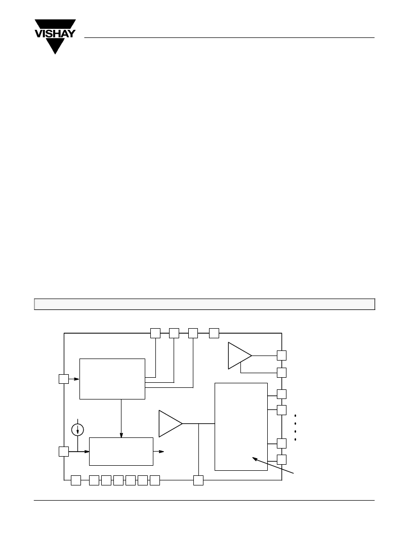
FUNCTIONAL BLOCK DIAGRAM
See
Functional Diagrams
(Page 6) for detailed descriptions
of SCSI Terminator Impedance
Circuits in LVD and S/E modes of
operation.
17
21
35
34
33
36
Heat Sink GND Pins
GND
REG
1.3 V
8
9
10
26
27
28
1
18
Enable
Current Limited
Source/Sink
Regulator
Comparators
V
V
V
0.5 = S/E
1.9 = LVD
2.4 = HPD
0.7
HPD
LVD
S/E
TERMPWR
20
19
5
4
32
31
Current Limited
Source/Sink
Regulator
Mode Control And
Enable/Disable
Circuitry
SCSI
Terminator
Impedance
Circuits
10 A
MODE
DISABLE
DIFFS
MSTR/SLV
T1N
T1P
T9P
T9N
相關PDF資料 |
PDF描述 |
|---|---|
| 73120 | N-Channel 25-V (D-S) MOSFET |
| 7314 | DIGITAL CONTROLLED AUDIO PROCESSOR WITH LOUDNESS |
| 7314 | AC POWER CONTROLLERS |
| 7314 | Low-Voltage, 10-Bit Digital Temperature Sensor in 8-Lead uSOIC |
| 73224 | N- and P-Channel 40-V (D-S) MOSFET |
相關代理商/技術參數 |
參數描述 |
|---|---|
| 73007 BRWN 1"X150' | 功能描述:SCOTCHCAL STRIPING TAPE 制造商:3m 系列:* 零件狀態:在售 標準包裝:1 |
| 73007-001 | 功能描述:DIN 41612 連接器 556-5FPF-DIN PCB ACCESSORIES E/// RoHS:否 制造商:HARTING 系列:har-bus 64 產品類型:Plugs 排數:5 位置/觸點數量:160 安裝角:Right 類型:Shrouded Header 端接類型:Solder 外殼材料: 觸點材料: 觸點電鍍: |
| 73007-001LF | 制造商:FCI 功能描述: |
| 7300-75 | 制造商:WAKEFIELD-VETTE 功能描述:EXTRUDED HEAT SINK |
| 73007W 008100 | 功能描述:CBL 7COND 20AWG 制造商:belden inc. 系列:* 零件狀態:在售 標準包裝:1 |
發布緊急采購,3分鐘左右您將得到回復。