- 您現在的位置:買賣IC網 > PDF目錄360436 > 74F410 (National Semiconductor Corporation) Register Stacká16 x 4 RAM TRI-STATEE Output Register PDF資料下載
參數資料
| 型號: | 74F410 |
| 廠商: | National Semiconductor Corporation |
| 英文描述: | Register Stacká16 x 4 RAM TRI-STATEE Output Register |
| 中文描述: | 注冊Stacká16 × 4內存三STATEE輸出寄存器 |
| 文件頁數: | 1/5頁 |
| 文件大小: | 52K |
| 代理商: | 74F410 |
Philips Semiconductors FAST Products
Product specification
74F410
Register stack – 16
×
4 RAM 3-State output register
1
January 8, 1990
853-1310 98498
FEATURES
Edge triggered output register
ypical access time of 19.5ns
Optimize for register stack operation
3–state outputs
18–pin package
DESCRIPTION
The 74F410 is a register oriented high speed
64–bit read/write memory organized as
16–words by 4–bits. An edge–triggered 4–bit
output register allows new input data to be
written while previous data is held. 3–state
outputs are provided for maximum versatility.
The 74F410 is fully compatible with all TTL
families.
TYPE
TYPICAL
ACCESS
TIME
TYPICAL
SUPPLY
CURRENT
( TOTAL)
74F410
19.5ns
45mA
FUNCTIONAL DESCRIPTION
Write operation
– When the three control
inputs, write enable (WE), chip select (CS),
and clock (CP), are low the information on
the data inputs (D0–D3) is written into the
memory location selected by the address
inputs (A0–A3). If the input data changes
while WE, CS, and CP are low, the contents
of the selected memory location follow these
changes provided setup and hold time criteria
are met.
Read operation
– When CS is low, WE is
high, and CP goes from low–to–high, the
contents of the memory location selected by
the address inputs (A0–A3) are edge–
triggered into the output register.
When WE is low, CS is low, CP goes from
low–to–high, the data at the data inputs is
edge–triggered into the output register. The
OE input controls the output buffers. When
OE is high the four outputs (Q0–Q3) are in a
high impedance or off state; when OE is low,
the outputs are determined by the state of the
output register.
ORDERING INFORMATION
ORDER CODE
DESCRIPTION
COMMERCIAL RANGE
V
CC
= 5V
±
10%, T
amb
= 0
°
C to +70
°
C
18–pin plastic DIP (300mil)
N74F410N
INPUT AND OUTPUT LOADING AND FAN OUT TABLE
PINS
DESCRIPTION
74F (U.L.)
HIGH/LOW
LOAD VALUE
HIGH/LOW
D0 – D3
Data inputs
1.0/1.0
20
μ
A
/
0.6mA
20
μ
A
/
0.6mA
20
μ
A/1.2mA
20
μ
A/1.2mA
20
μ
A/0.6mA
20
μ
A/0.6mA
A0 – A3
Address inputs
1.0/1.0
CP
Clock pulse input (active rising edge)
1.0/2.0
CS
Chip select input (active low)
1.0/2.0
OE
Output enable input (active low)
1.0/1.0
WE
Write enable input (active low)
1.0/1.0
Q0 – Q3
Data outputs
150/40
3mA/24mA
NOTE:
One (1.0) FAST unit load is defined as: 20
μ
A in the high state and 0.6mA in the low state.
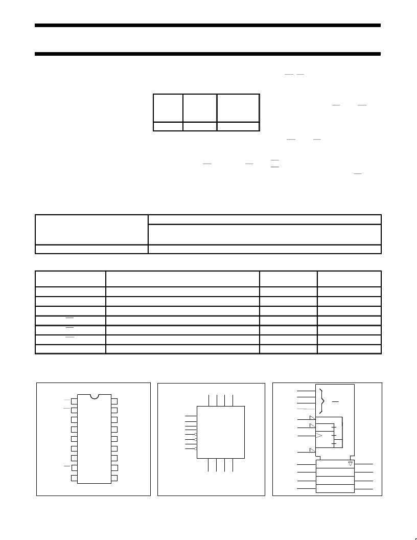
PIN CONFIGURATION
LOGIC SYMBOL
IEC/IEEE SYMBOL
18
17
16
15
14
13
12
7
6
5
4
3
2
1
A1
Q1
Q2
D3
D2
D0
Q0
CS
WE
CP
A0
A3
OE
3
4
5
6
11
10
D0
D2 D3
D1
Q0 Q1 Q2 Q3
16 14 12 10
15 13 11
11
8
A2
V
CC
V
= Pin 18
GND = Pin 9
D1
17
A0
A1
A2
A3
CS
WE
CP
OE
3
4
5
6
1
2
7
8
13
12
15
14
17
16
2
1
A1,2D
A3
&
0
1
A0
15
Q3
GND
10
9
7
8
&
G1
G2
1C
EN3
相關PDF資料 |
PDF描述 |
|---|---|
| 74F412DC | 8-Bit D-Type Latch |
| 54F410DMQB | REGISTER FILE|F-TTL|DIP|18PIN|CERAMIC |
| 54F410FMQB | REGISTER FILE|F-TTL|FP|CERAMIC |
| 54F410LMQB | REGISTER FILE|F-TTL|LLCC|20PIN|CERAMIC |
| 54F412DM | Logic IC |
相關代理商/技術參數 |
參數描述 |
|---|---|
| 74F410DC | 制造商:PHILIPS 制造商全稱:NXP Semiconductors 功能描述:Register File |
| 74F410PC | 制造商:NSC 制造商全稱:National Semiconductor 功能描述:Register Stacká16 x 4 RAM TRI-STATEE Output Register |
| 74F410SC | 制造商:NSC 制造商全稱:National Semiconductor 功能描述:Register Stacká16 x 4 RAM TRI-STATEE Output Register |
| 74F412DC | 制造商:未知廠家 制造商全稱:未知廠家 功能描述:8-Bit D-Type Latch |
| 74F412PC | 制造商:未知廠家 制造商全稱:未知廠家 功能描述:8-Bit D-Type Latch |
發布緊急采購,3分鐘左右您將得到回復。