- 您現在的位置:買賣IC網 > PDF目錄369304 > 74FCT162827CTPVCT (Texas Instruments, Inc.) 20-Bit Buffers/Line Drivers PDF資料下載
參數資料
| 型號: | 74FCT162827CTPVCT |
| 廠商: | Texas Instruments, Inc. |
| 英文描述: | 20-Bit Buffers/Line Drivers |
| 中文描述: | 20位緩沖器/線路驅動器 |
| 文件頁數: | 1/7頁 |
| 文件大小: | 62K |
| 代理商: | 74FCT162827CTPVCT |
20-Bit Buffers/Line Drivers
CY74FCT16827T
CY74FCT162827T
Data sheet acquired from Cypress Semiconductor Corporation.
Data sheet modified to remove devices not offered.
SCCS064 - August 1994 - Revised March 2000
Copyright
2000, Texas Instruments Incorporated
1CY74FCT162827T
Features
FCT-E speed at 3.2 ns
Power-off disable outputs permits live insertion
Edge-rate control circuitry for significantly improved
noise characteristics
Typical output skew < 250 ps
ESD > 2000V
TSSOP (19.6-mil pitch) and SSOP (25-mil pitch)
packages
Industrial temperature range of
40C to +85C
V
CC
= 5V
±
10%
CY74FCT16827T Features:
64 mA sink current, 32 mA source current
Typical V
OLP
(ground bounce) <1.0V at V
CC
= 5V,
T
A
= 25C
CY74FCT162827T Features:
Balanced 24 mA output drivers
Reduced system switching noise
Typical V
OLP
(ground bounce) <0.6V at V
CC
= 5V,
T
A
= 25C
Functional Description
The CY74FCT16827T 20-bit buffer/line driver and the
CY74FCT162827T
20-bit
high-performance bus interface buffering for wide data/address
pathsorbusescarryingparity.Thesepartscanbeusedasasingle
20-bit buffer or two 10-bit buffers. Each 10-bit buffer has a pair of
NANDedOEforincreasedflexibility.Theoutputsaredesignedwith
a power-off disable feature to allow for live insertion of boards.
The
CY74FCT16827T
is
high-capacitance loads and low-impedance backplanes.
The CY74FCT162827T has 24-mA balanced output drivers
with current-limiting resistors in the outputs. This reduces the
need for external terminating resistors and provides for
minimal undershoot and reduced ground bounce. The
CY74FCT162827T is ideal for driving transmission lines.
buffer/line
driver
provide
ideally
suited
for
driving
GND
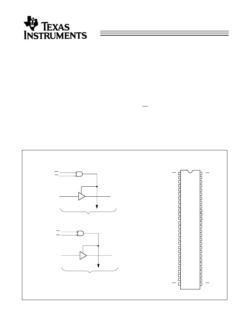
Logic Block Diagrams
Pin Configuration
1
2
3
4
5
6
7
8
9
10
11
12
13
33
32
31
30
29
36
35
1
OE
1
1
Y
1
1
Y
2
GND
34
SSOP/TSSOP
Top View
1
Y
1
14
15
16
17
18
19
20
21
22
23
24
25
45
44
43
42
41
37
38
39
40
48
47
46
1
A
1
1
OE
1
1
OE
2
1
Y
3
1
Y
4
V
CC
1
Y
5
1
Y
6
1
Y
7
1
A
1
1
A
2
1
A
3
1
A
4
V
CC
1
A
5
1
OE
2
GND
1
A
8
2
Y
3
GND
2
Y
4
2
Y
5
2
Y
6
2
Y
1
2
Y
2
1
A
6
GND
1
Y
8
2
OE
1
FCT16827-1
TO 9 OTHER CHANNELS
2
A
1
2
OE
1
2
OE
2
TO 9 OTHER CHANNELS
2
Y
1
1
Y
9
1
Y
10
2
Y
9
2
Y
10
2
Y
7
2
Y
8
GND
V
CC
26
27
28
55
54
53
52
51
50
49
56
1
A
7
1
A
9
1
A
10
2
A
3
GND
2
A
4
2
A
5
2
A
6
2
A
2
2
A
9
2
A
10
2
OE
2
2
A
7
2
A
8
GND
V
CC
2
A
1
FCT16827-2
FCT16827-3
相關PDF資料 |
PDF描述 |
|---|---|
| 74FCT162841 | 20-Bit Latches |
| 74FCT162841CTPVCT | 20-Bit Latches |
| 74FCT162H245ATPVCT | 16-bIT TRANSCEI |
| 74FCT16245 | 16-bIT TRANSCEI |
| 74FCT162H543CTPACT | 16-Bit Latched Transceivers |
相關代理商/技術參數 |
參數描述 |
|---|---|
| 74FCT162827CTPVG | 功能描述:緩沖器和線路驅動器 RoHS:否 制造商:Micrel 輸入線路數量:1 輸出線路數量:2 極性:Non-Inverting 電源電壓-最大:+/- 5.5 V 電源電壓-最小:+/- 2.37 V 最大工作溫度:+ 85 C 安裝風格:SMD/SMT 封裝 / 箱體:MSOP-8 封裝:Reel |
| 74FCT162827CTPVG8 | 功能描述:緩沖器和線路驅動器 RoHS:否 制造商:Micrel 輸入線路數量:1 輸出線路數量:2 極性:Non-Inverting 電源電壓-最大:+/- 5.5 V 電源電壓-最小:+/- 2.37 V 最大工作溫度:+ 85 C 安裝風格:SMD/SMT 封裝 / 箱體:MSOP-8 封裝:Reel |
| 74FCT162827ETPACT | 制造商:TI 制造商全稱:Texas Instruments 功能描述:20-Bit Buffers/Line Drivers |
| 74FCT162827ETPVCT | 制造商:Rochester Electronics LLC 功能描述:- Bulk |
| 74FCT162827NATPA | 制造商:Integrated Device Technology Inc 功能描述: |
發布緊急采購,3分鐘左右您將得到回復。