- 您現在的位置:買賣IC網 > PDF目錄352323 > 74LS298 (Texas Instruments, Inc.) QUADRUPLE 2-INPUT MULTIPLEXERS WITH STORAGE PDF資料下載
參數資料
| 型號: | 74LS298 |
| 廠商: | Texas Instruments, Inc. |
| 英文描述: | QUADRUPLE 2-INPUT MULTIPLEXERS WITH STORAGE |
| 中文描述: | 四2輸入多路復用器與存儲 |
| 文件頁數: | 1/4頁 |
| 文件大小: | 43K |
| 代理商: | 74LS298 |
2000 Fairchild Semiconductor Corporation
DS009826
www.fairchildsemi.com
October 1988
Revised March 2000
DM74LS298
Quad
2-Por
tRegist
er
Mult
ipl
exer
wit
h
S
tora
g
e
DM74LS298
Quad 2-Port Register Multiplexer with Storage
General Description
The DM74LS298 is a quad 2-port register. It is the logical
equivalent of a quad 2-input multiplexer followed by a quad
4-bit edge-triggered register. A Common Select input
selects between two 4-bit input ports (data sources). The
selected data is transferred to the output register synchro-
nous with the HIGH-to-LOW transition of the Clock input.
Features
s Select from two data sources
s Fully edge-triggered operation
s Typical power dissipation of 65 mW
Ordering Code:
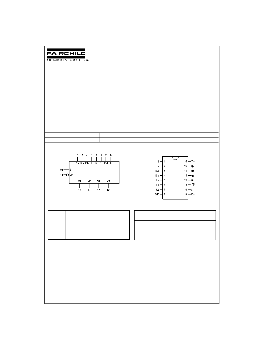
Logic Symbol
VCC = Pin 16
GND
= Pin 8
Pin Descriptions
Connection Diagram
Truth Table
l
= LOW Voltage Level one setup time prior to the HIGH-to-LOW clock
transition.
h
= HIGH Voltage Level one setup time prior to the HIGH-to-LOW clock
transition.
H
= HIGH Voltage Level
L
= LOW Voltage Level
X
= Immaterial
Order Number
Package Number
Package Description
DM74LS298N
N16E
16-Lead Plastic Dual-In-Line Package (PDIP), JEDEC MS-001, 0.300 Wide
Pin Names
Description
S
Common Select Inputs
CP
Clock Pulse Input (Active Falling Edge)
I0a, I0d
Source 0 Data Inputs
I1a, I1d
Source 1 Data Inputs
Qa, Qd
Flip-Flip Outputs
Inputs
Output
SI0x
I1x
Qx
ll
X
L
lh
X
H
hX
l
L
hX
h
H
相關PDF資料 |
PDF描述 |
|---|---|
| 74LS30 | 8-INPUT POSITIVE-NAND GATES |
| 74LS30N | 8-INPUT POSITIVE-NAND GATES |
| 74LS32 | QUADRUPLE 2-INPUT POSITIVE-OR GATES |
| 74LS645 | OCTAL BUS TRANSCEIVERS |
| 74LS670 | 4-BY-4 REGISTER FILES WITH 3-STATE OUTPUTS |
相關代理商/技術參數 |
參數描述 |
|---|---|
| 74LS298 WAF | 制造商:Fairchild Semiconductor Corporation 功能描述: |
| 74LS298DC | 制造商:Rochester Electronics LLC 功能描述:- Bulk |
| 74LS298N 90 | 制造商:Motorola 功能描述:74LS298N |
| 74LS298N90 | 制造商:Motorola 功能描述:74LS298N |
| 74LS298PC | 制造商:Rochester Electronics LLC 功能描述:- Bulk |
發布緊急采購,3分鐘左右您將得到回復。