- 您現在的位置:買賣IC網 > PDF目錄369318 > 74LVC2G08GM (Panasonic Corporation) Hex Buffers And Line Drivers With 3-State Outputs 16-SOIC -40 to 85 PDF資料下載
參數資料
| 型號: | 74LVC2G08GM |
| 廠商: | Panasonic Corporation |
| 英文描述: | Hex Buffers And Line Drivers With 3-State Outputs 16-SOIC -40 to 85 |
| 中文描述: | 3態輸出六緩沖線性驅動器 SOIC-16封裝 工作溫度:-40℃_85℃ |
| 文件頁數: | 2/15頁 |
| 文件大小: | 87K |
| 代理商: | 74LVC2G08GM |
2004 Sep 15
2
Philips Semiconductors
Product specification
Dual 2-input AND gate
74LVC2G08
FEATURES
Wide supply voltage range from 1.65 V to 5.5 V
5 V tolerant inputs and outputs for interfacing with 5 V
logic
High noise immunity
Complies with JEDEC standard:
– JESD8-7 (1.65 V to 1.95 V)
– JESD8-5 (2.3 V to 2.7 V)
– JESD8B/JESD36 (2.7 V to 3.6 V).
±
24 mA output drive (V
CC
= 3.0 V)
CMOS low power consumption
Latch-up performance exceeds 250 mA
Direct interface with TTL levels
Inputs accept voltages up to 5 V
Multiple packages options
ESD protection:
– HBM EIA/JESD22-A114-B exceeds 2000 V
– MM EIA/JESD22-A115-A exceeds 200 V.
Specified from
40
°
C to +85
°
C and
40
°
C to +125
°
C.
DESCRIPTION
The 74LVC2G08 is a high-performance, low-power,
low-voltage, Si-gate CMOS device and superior to most
advanced CMOS compatible TTL families.
Inputs can be driven from either 3.3 V or 5 V devices. This
feature allows the use of these devices as translators in a
mixed 3.3 V and 5 V environment.
This device is fully specified for partial power-down
applications using I
off
. The I
off
circuitry disables the output,
preventing the damaging backflow current through the
device when it is powered down.
The 74LVC2G08 provides the 2-input AND gate function.
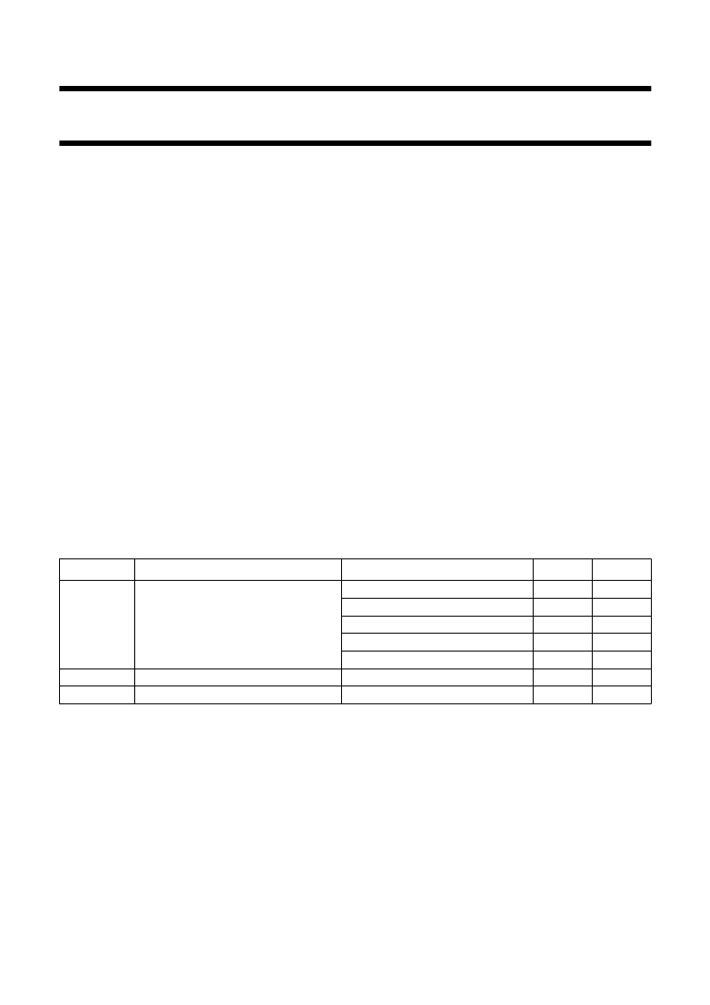
QUICK REFERENCE DATA
GND = 0 V; T
amb
= 25
°
C; t
r
= t
f
≤
2.5 ns.
Notes
1.
C
PD
is used to determine the dynamic power dissipation (P
D
in
μ
W).
P
D
= C
PD
×
V
CC2
×
f
i
×
N +
∑
(C
L
×
V
CC2
×
f
o
) where:
f
i
= input frequency in MHz;
f
o
= output frequency in MHz;
C
L
= output load capacitance in pF;
V
CC
= supply voltage in Volts;
N = total load switching outputs;
∑
(C
L
×
V
CC2
×
f
o
) = sum of outputs.
The condition is V
I
= GND to V
CC
.
2.
SYMBOL
PARAMETER
CONDITIONS
TYPICAL
UNIT
t
PHL
/t
PLH
propagation delay inputs nA, nB to
outputs nY
V
CC
= 1.8 V; C
L
= 30 pF; R
L
= 1 k
V
CC
= 2.5 V; C
L
= 30 pF; R
L
= 500
2.2
V
CC
= 2.7 V; C
L
= 50 pF; R
L
= 500
2.5
V
CC
= 3.3 V; C
L
= 50 pF; R
L
= 500
2.1
V
CC
= 5.0 V; C
L
= 50 pF; R
L
= 500
1.7
3.2
ns
ns
ns
ns
ns
pF
pF
C
I
C
PD
input capacitance
power dissipation capacitance per gate
2.5
14.4
V
CC
= 3.3 V; notes 1 and 2
相關PDF資料 |
PDF描述 |
|---|---|
| 74LVQ00T | QUAD 2-INPUT NAND GATE |
| 74LVQ00M | QUAD 2-INPUT NAND GATE |
| 74LVQ00SJ | Low Voltage Quad 2-Input NAND Gate |
| 74LVQ00SJX | 16 characters x 4 Lines, 5x7 Dot Matric Character and Cursor |
| 74LVQ00 | Low Voltage Quad 2-Input NAND Gate |
相關代理商/技術參數 |
參數描述 |
|---|---|
| 74LVC2G08GM,125 | 功能描述:邏輯門 3.3V DUAL 2-INPUT AND GATE RoHS:否 制造商:Texas Instruments 產品:OR 邏輯系列:LVC 柵極數量:2 線路數量(輸入/輸出):2 / 1 高電平輸出電流:- 16 mA 低電平輸出電流:16 mA 傳播延遲時間:3.8 ns 電源電壓-最大:5.5 V 電源電壓-最小:1.65 V 最大工作溫度:+ 125 C 安裝風格:SMD/SMT 封裝 / 箱體:DCU-8 封裝:Reel |
| 74LVC2G08GN | 制造商:NXP Semiconductors 功能描述:Bulk 制造商:NXP Semiconductors 功能描述:IC DUAL 2 INPUT AND GATE XS |
| 74LVC2G08GN,115 | 功能描述:邏輯門 Dual 2-input AND gate RoHS:否 制造商:Texas Instruments 產品:OR 邏輯系列:LVC 柵極數量:2 線路數量(輸入/輸出):2 / 1 高電平輸出電流:- 16 mA 低電平輸出電流:16 mA 傳播延遲時間:3.8 ns 電源電壓-最大:5.5 V 電源電壓-最小:1.65 V 最大工作溫度:+ 125 C 安裝風格:SMD/SMT 封裝 / 箱體:DCU-8 封裝:Reel |
| 74LVC2G08GS,115 | 功能描述:轉換 - 電壓電平 11.3ns 5.5V 300mW RoHS:否 制造商:Micrel 類型:CML/LVDS/LVPECL to LVCMOS/LVTTL 傳播延遲時間:1.9 ns 電源電流:14 mA 電源電壓-最大:3.6 V 電源電壓-最小:3 V 最大工作溫度:+ 85 C 安裝風格:SMD/SMT 封裝 / 箱體:MLF-8 |
| 74LVC2G08GT | 制造商:NXP Semiconductors 功能描述:IC DUAL 2 INPUT AND GATE XS |
發布緊急采購,3分鐘左右您將得到回復。