- 您現在的位置:買賣IC網 > PDF目錄369325 > 74S225 (Texas Instruments, Inc.) 16 】 5 ASYNCHRONOUS FIRST-IN, FIRST-OUT MEMORY WITH 3-STATE OUTPUTS PDF資料下載
參數資料
| 型號: | 74S225 |
| 廠商: | Texas Instruments, Inc. |
| 英文描述: | 16 】 5 ASYNCHRONOUS FIRST-IN, FIRST-OUT MEMORY WITH 3-STATE OUTPUTS |
| 中文描述: | 16】5異步先入先出3記憶態(tài)輸出 |
| 文件頁數: | 1/10頁 |
| 文件大小: | 145K |
| 代理商: | 74S225 |
SN74S225
16
×
5 ASYNCHRONOUS FIRST-IN, FIRST-OUT MEMORY
WITH 3-STATE OUTPUTS
SDLS207B – SEPTEMBER 1976 – REVISED APRIL 1998
1
POST OFFICE BOX 655303
DALLAS, TEXAS 75265
Independent Asychronous Inputs and
Outputs
16 Words by 5 Bits
DC to 10-MHz Data Rate
3-State Outputs
Packaged in Standard Plastic 300-mil DIPs
description
This 80-bit active-element memory is a monolithic
Schottky-clamped
transistor-transistor
(STTL) array organized as 16 words by 5 bits. A
memory system using the SN74S225 easily can
be expanded in multiples of 48 words or of 10 bits
as shown in Figure 3. The 3-state outputs
controlled by a single output-enable (OE) input
make bus connection and multiplexing easy.
logic
A first-in, first-out (FIFO) memory is a storage device that allows data to be written into and read from its array
at independent data rates. This FIFO is designed to process data at rates from dc to 10 MHz in a bit-parallel
format, word by word.
Reading or writing is done independently, utilizing separate asynchronous data clocks. Data can be written into
the array on the low-to-high transition of either load-clock (CLKA, CLKB) input. Data can be read out of the array
on the low-to-high transition of the unload-clock (UNCK IN) input (normally high). Writing data into the FIFO can
be accomplished in one of two ways:
In applications not requiring a gated clock control, best results are achieved by applying the clock input to
one of the clocks while tying the other clock input high.
In applications needing a gated clock, the load clock (gate control) must be high for the FIFO to load on the
next clock pulse.
CLKA and CLKB can be used interchangeably for either clock gate control or clock input.
Status of the SN74S225 is provided by three outputs. The input-ready (IR) output monitors the status of the last
word location and signifies when the memory is full. This output is high whenever the memory is available to
accept any data. The unload-clock (UNCK OUT) output also monitors the last word location. This output
generates a low-logic-level pulse (synchronized to the internal clock pulse) when the location is vacant. The third
status output, output ready (OR), is high when the first word location contains valid data and UNCK IN is high.
When UNCK IN goes low, OR will go low and stay low until new valid data is in the first word position. The first
word location is defined as the location from which data is provided to the outputs.
The data outputs are noninverted with respect to the data inputs and are 3-state, with a common control input
(OE). When OE is low, the data outputs are enabled to function as totem-pole outputs. A high logic level forces
each data output to a high-impedance state while all other inputs and outputs remain active.The clear (CLR)
input invalidates all data stored in the memory array by clearing the control logic and setting OR to a low logic
level on the high-to-low transition of a low-active pulse.
The SN74S225 is characterized for operation from 0
°
C to 70
°
C.
Copyright
1998, Texas Instruments Incorporated
PRODUCTION DATA information is current as of publication date.
Products conform to specifications per the terms of Texas Instruments
standard warranty. Production processing does not necessarily include
testing of all parameters.
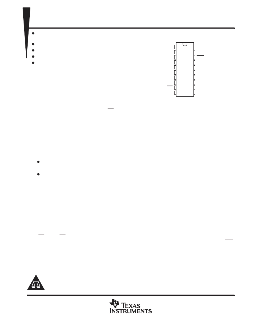
1
2
3
4
5
6
7
8
9
10
20
19
18
17
16
15
14
13
12
11
CLKA
IR
UNCK OUT
D0
D1
D2
D3
D4
OE
GND
V
CC
CLKB
CLR
OR
UNCK IN
Q0
Q1
Q2
Q3
Q4
N PACKAGE
(TOP VIEW)
Please be aware that an important notice concerning availability, standard warranty, and use in critical applications of
Texas Instruments semiconductor products and disclaimers thereto appears at the end of this data sheet.
相關PDF資料 |
PDF描述 |
|---|---|
| 74S289 | 64BIT RANDOM ACCESS MEMORY |
| 74LS289 | 64BIT RANDOM ACCESS MEMORY |
| 74S299 | 8-BIT UNIVERSAL SHIFT/STORAGE REGISTERS |
| 74S473 | (512 x 8) 4096-Bit TTL PROM |
| 74V1G00 | SINGLE 2-INPUT NAND GATE |
相關代理商/技術參數 |
參數描述 |
|---|---|
| 74S225AJ | 制造商:未知廠家 制造商全稱:未知廠家 功能描述:x5 Asynchronous FIFO |
| 74S225AN | 制造商:未知廠家 制造商全稱:未知廠家 功能描述:x5 Asynchronous FIFO |
| 74S225J | 制造商:未知廠家 制造商全稱:未知廠家 功能描述:x5 Asynchronous FIFO |
| 74S225N | 制造商:SNT 功能描述: 制造商:North American Philips Discrete Products Div 功能描述:FIFO, 16 x 5, Asynchronous, 20 Pin, Plastic, DIP 制造商:NXP Semiconductors 功能描述:FIFO, 16 x 5, Asynchronous, 20 Pin, Plastic, DIP 制造商:Texas Instruments 功能描述:FIFO, 16 x 5, Asynchronous, 20 Pin, Plastic, DIP |
| 74S226J | 制造商:Rochester Electronics LLC 功能描述:- Bulk |
發(fā)布緊急采購,3分鐘左右您將得到回復。