- 您現在的位置:買賣IC網 > PDF目錄360547 > 7HCPL-5230-200 Hermetically Sealed, Low IF, Wide VCC, Logic Gate Optocouplers PDF資料下載
參數資料
| 型號: | 7HCPL-5230-200 |
| 英文描述: | Hermetically Sealed, Low IF, Wide VCC, Logic Gate Optocouplers |
| 中文描述: | 密封,中頻,寬虛擬通道連接,低邏輯門光電耦合器 |
| 文件頁數: | 1/12頁 |
| 文件大小: | 294K |
| 代理商: | 7HCPL-5230-200 |
Hermetically Sealed,
Low I
F
, Wide V
CC
,
Logic Gate Optocouplers
Technical Data
Features
Dual Marked with Device
Part Number and DSCC
Standard Microcircuit
Drawing
Manufactured and Tested on
a MIL-PRF-38534 Certified
Line
QML-38534, Class H and K
Four Hermetically Sealed
Package Configurations
Performance Guaranteed
over -55
°
C to +125
°
C
Wide V
CC
Range (4.5 to 20 V)
350 ns Maximum Propaga-
tion Delay
CMR: > 10,000 V/
μ
s Typical
1500 Vdc Withstand Test
Voltage
Three State Output Available
High Radiation Immunity
HCPL-2200/31 Function
Compatibility
Reliability Data Available
Compatible with LSTTL,
TTL, and CMOS Logic
Applications
Military and Space
High Reliability Systems
Transportation and Life
Critical Systems
High Speed Line Receiver
CAUTION: It is advised that normal static precautions be taken in handling and assembly of this component to
prevent damage and/or degradation which may be induced by ESD.
Isolated Bus Driver (Single
Channel)
Pulse Transformer
Replacement
Ground Loop Elimination
Harsh Industrial
Environments
Computer-Peripheral
Interfaces
Description
These units are single, dual and
quad channel, hermetically sealed
optocouplers. The products are
capable of operation and storage
over the full military temperature
range and can be purchased as
either standard product or with
full MIL-PRF-38534 Class Level
H or K testing or from the
appropriate DSCC Drawing. All
devices are manufactured and
tested on a MIL-PRF-38534
certified line and are included in
the DSCC Qualified Manufac-
turers List QML-38534 for Hybrid
Microcircuits.
Each channel contains an AlGaAs
light emitting diode which is
optically coupled to an integrated
high gain photon detector. The
detector has a threshold with
hysteresis which provides differ-
ential mode noise immunity and
eliminates the potential for
output signal chatter. The
detector in the single channel
units has a tri-state output stage
Truth Tables
(Positive Logic)
Multichannel Devices
Input
On (H)
Off (L)
Output
H
L
HCPL-520x*
5962-88768
HCPL-523x
HCPL-623x
HCPL-625x
5962-88769
*See matrix for available extensions.
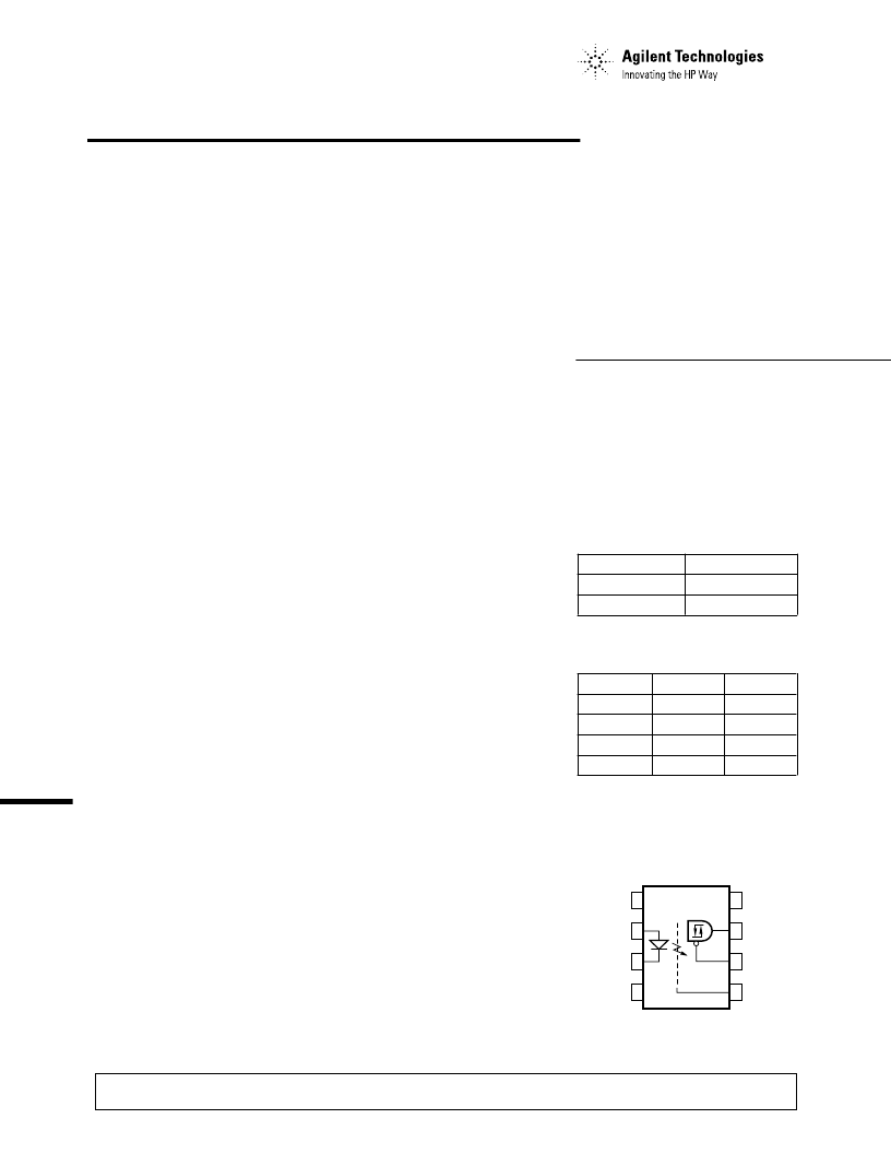
Functional Diagram
Multiple Channel Devices
Available
V
CC
V
O
V
E
GND
Single Channel DIP
Input
On (H)
Off (L)
On (H)
Off (L)
Enable
H
H
L
L
Output
Z
Z
H
L
A 0.1
μ
F bypass capacitor must be connected between V
CC
and GND pins.
相關PDF資料 |
PDF描述 |
|---|---|
| 7HCT1284D | Parallel printer interface transceiver/buffer |
| 7LN115 | Optoelectronic |
| 7LVC125APWDH | SC Series, 3 Ohms, 1.0 W, Fixed, Wirewound Resistor |
| 7LVC1284D | 3.3V Parallel printer interface transceiver/buffer |
| 7LVC240APWDH | Octal buffer/line driver with 5-volt tolerant inputs/outputs; inverting 3-State |
相關代理商/技術參數 |
參數描述 |
|---|---|
| 7HCT1284D | 制造商:PHILIPS 制造商全稱:NXP Semiconductors 功能描述:Parallel printer interface transceiver/buffer |
| 7HDD15SAR99E20X | 功能描述:15P F HD PC WATER RES 制造商:conec 系列:* 零件狀態:有效 標準包裝:30 |
| 7HG8 | 制造商:Misc 功能描述: 制造商:Tubes 功能描述: |
| 7HI800013000 | 制造商:Eurotherm Inc 功能描述:DIGITAL PANEL INDICATOR WITH LINEAR DC THERMOCOUPLE & RTD INPUT100/240 VAC WITH |
| 7HM5 | 功能描述:基本/快動開關 SPDT 1A 28VDC BASIC SWITCH RoHS:否 制造商:Omron Electronics 觸點形式:SPDT 執行器:Lever 電流額定值:5 A 電壓額定值 AC:250 V 電壓額定值 DC:30 V 功率額定值: 工作力:120 g IP 等級:IP 67 NEMA 額定值: 端接類型:Wire 安裝:Panel |
發布緊急采購,3分鐘左右您將得到回復。