- 您現在的位置:買賣IC網 > PDF目錄250212 > 7P16FLE210C15 (WHITE ELECTRONIC DESIGNS CORP) 8M X 16 FLASH 5V PROM CARD, 150 ns, UUC68 PDF資料下載
參數資料
| 型號: | 7P16FLE210C15 |
| 廠商: | WHITE ELECTRONIC DESIGNS CORP |
| 元件分類: | PROM |
| 英文描述: | 8M X 16 FLASH 5V PROM CARD, 150 ns, UUC68 |
| 封裝: | CARD-68 |
| 文件頁數: | 9/13頁 |
| 文件大小: | 238K |
| 代理商: | 7P16FLE210C15 |
5
White Electronic Designs Corporation (602) 437-1520 www.whiteedc.com
White Electronic Designs
PCMCIA Flash Memory Card
FLE Series
August 2000
Rev. 4
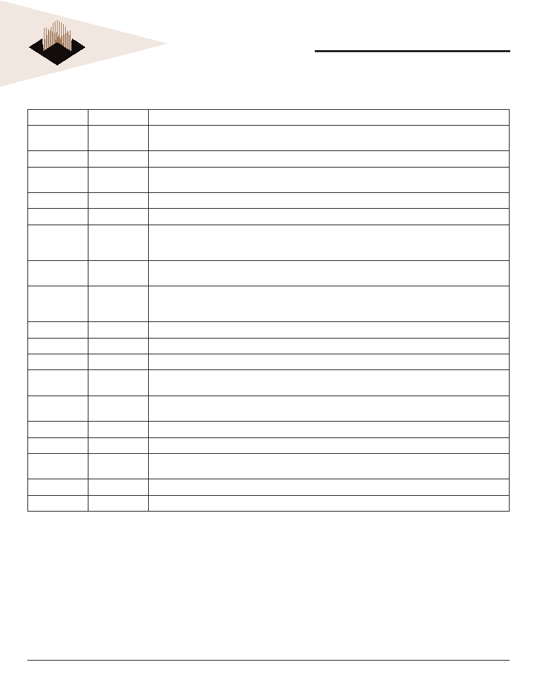
CARD SIGNAL DESCRIPTION
Symbol
Type
Name and Function
A0 - A25
INPUT
ADDRESS INPUTS: A0 through A25 enable direct addressing of up to 64MB of memory on the card. Signal A0 is not
used in word access mode. A25 is the most signicant bit
DQ0 - DQ15
INPUT/OUTPUT
DATA INPUT/OUTPUT: DQ0 THROUGH DQ15 constitute the bi-directional databus. DQ15 is the MSB.
CE1#, CE2#
INPUT
CARD ENABLE 1 AND 2: CE1# enables even byte accesses, CE2# enables odd byte accesses. Multiplexing A0,
CE1# and CE2# allows 8-bit hosts to access all data on DQ0 - DQ7.
OE#
INPUT
OUTPUT ENABLE: Active low signal gating read data from the memory card.
WE#
INPUT
WRITE ENABLE: Active low signal gating write data to the memory card.
RDY/BSY#
OUTPUT
READY/BUSY OUTPUT: Indicates status of internally timed erase or program algorithms. A high output indicates that
the card is ready to accept accesses. A low output indicates that one or more devices in the memory card are busy
with internally timed erase or write activities.
CD1#, CD2#
OUTPUT
CARD DETECT 1 and 2: Provide card insertion detection. These signals are connected to ground internally on the
memory card. The host socket interface circuitry shall supply 10K-ohm or larger pull-up resistors on these signal pins.
WP
OUTPUT
WRITE PROTECT: Write protect reects the status of the Write Protect switch on the memory card. WP set to high
= write protected, providing internal hardware write lockout to the Flash array. If card does not include optional write
protect switch, this signal will be pulled low internally indicating write protect = “off”.
VPP1, VPP2
N.C.
PROGRAM/ERASE POWER SUPPLY: Not connected for 5V only card.
VCC
CARD POWER SUPPLY: 5.0V for all internal circuitry.
GND
GROUND: for all internal circuitry.
REG#
INPUT
ATTRIBUTE MEMORY SELECT: provides access to Flash memory card registers and Card Information Structure in
the Attribute Memory Plane.
RST
INPUT
RESET: Active high signal for placing card in Power-on default state. Reset can be used as a Power-Down signal for
the memory array.
WAIT#
OUTPUT
WAIT: This signal is pulled high internally for compatibility. No wait states are generated.
BVD1, BVD2
OUTPUT
BATTERY VOLTAGE DETECT: These signals are pulled high to maintain SRAM card compatibility.
VS1, VS2
OUTPUT
VOLTAGE SENSE: Noties the host socket of the card’s VCC requirements. VS1 and VS2 are open to indicate a 5V
card has been inserted.
RFU
RESERVED FOR FUTURE USE
N.C.
NO INTERNAL CONNECTION TO CARD: pin may be driven or left oating
相關PDF資料 |
PDF描述 |
|---|---|
| 7P48FLE222C25 | 32M X 16 FLASH 5V PROM CARD, 150 ns, UUC68 |
| 7P8FLE211C25 | 4M X 16 FLASH 5V PROM CARD, 150 ns, UUC68 |
| 70V659S10DR | 128K X 36 DUAL-PORT SRAM, 10 ns, PQFP208 |
| 7P12FLV262C25 | 6M X 16 FLASH 3V PROM CARD, 250 ns, XMA68 |
| 7P12FLV520I15 | 6M X 16 FLASH 3V PROM CARD, 150 ns, XMA68 |
相關代理商/技術參數 |
參數描述 |
|---|---|
| 7P-19.200MBP-T | 功能描述:19.2MHz Clipped Sine Wave, CMOS TCXO Oscillator Surface Mount 2.7 V ~ 5.5 V 10mA 制造商:txc corporation 系列:7P 包裝:剪切帶(CT) 零件狀態:有效 類型:TCXO 頻率:19.2MHz 功能:- 輸出:削峰正弦波,CMOS 電壓 - 電源:2.7 V ~ 5.5 V 頻率穩定度:±280ppb 工作溫度:-40°C ~ 85°C 電流 - 電源(最大值):10mA 等級:- 安裝類型:表面貼裝 大小/尺寸:0.197" 長 x 0.126" 寬(5.00mm x 3.20mm) 高度:0.065"(1.65mm) 封裝/外殼:6-SMD,無引線(DFN,LCC) 電流 - 電源(禁用)(最大值):- 標準包裝:1 |
| 7P20 | 制造商:UTC-IC 制造商全稱:UTC-IC 功能描述:200V P-CHANNEL MOSFET |
| 7P20_11 | 制造商:UTC-IC 制造商全稱:UTC-IC 功能描述:200V P-CHANNEL MOSFET |
| 7P202V330A082 | 制造商:CDE 制造商全稱:Cornell Dubilier Electronics 功能描述:Type 7P 55 ∑C Photoflash, High-Energy, Long Life, Aluminum |
| 7P202V330A082L | 制造商:Cornell Dubilier Electronics 功能描述:ALUMINUM ELECTROLYTIC CAPACITOR |
發布緊急采購,3分鐘左右您將得到回復。