- 您現在的位置:買賣IC網 > PDF目錄24610 > 9112AF-17 (INTEGRATED DEVICE TECHNOLOGY INC) 9112 SERIES, PLL BASED CLOCK DRIVER, 8 TRUE OUTPUT(S), 0 INVERTED OUTPUT(S), PDSO16 PDF資料下載
參數資料
| 型號: | 9112AF-17 |
| 廠商: | INTEGRATED DEVICE TECHNOLOGY INC |
| 元件分類: | 時鐘及定時 |
| 英文描述: | 9112 SERIES, PLL BASED CLOCK DRIVER, 8 TRUE OUTPUT(S), 0 INVERTED OUTPUT(S), PDSO16 |
| 封裝: | 0.150 INCH, MO-137, SSOP-16 |
| 文件頁數: | 1/12頁 |
| 文件大小: | 163K |
| 代理商: | 9112AF-17 |
Integrated
Circuit
Systems, Inc.
General Description
Features
ICS9112-17
0051J—02/05/04
Block Diagram
Low Skew Output Buffer
Pin Configuration
Zero input - output delay
Frequency range 25 - 133 MHz (3.3V)
High loop filter bandwidth ideal for Spread Spectrum
applications.
Less than 200 ps cycle to cycle Jitter
Skew controlled outputs
Skew less than 250 ps between outputs
Available in 16 pin, 150 mil SSOP & SOIC package
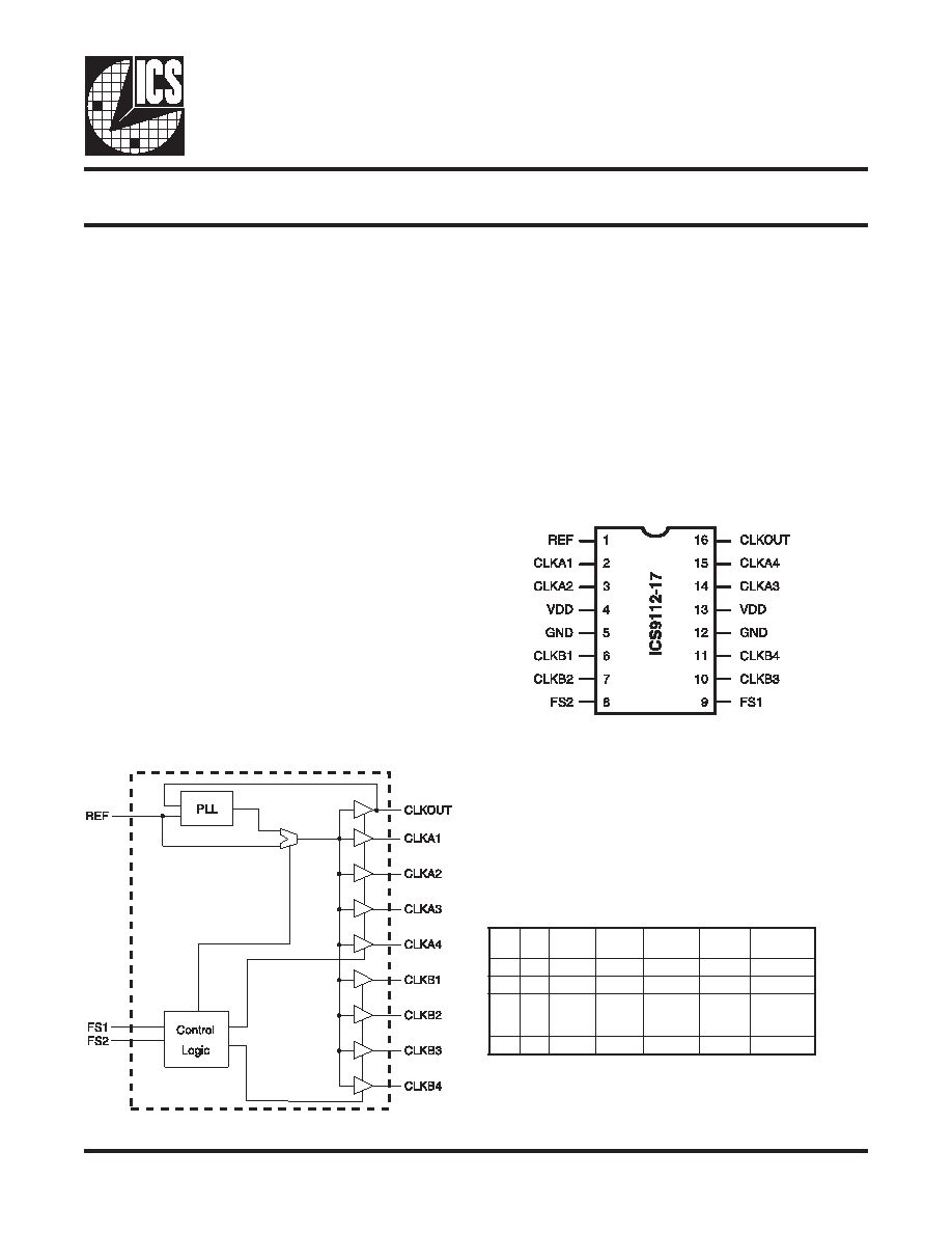
The ICS9112-17 is a high performance, low skew, low jitter
zero delay buffer.
It uses a phase lock loop (PLL)
technology to align, in both phase and frequency, the REF
input with the CLKOUT signal. It is designed to distribute
high speed clocks in PC systems operating at speeds
from 25 to 133 MHz.
ICS9112-17 is a zero delay buffer that provides
synchronization between the input and output. The
synchronization is established via CLKOUT feed back to
the input of the PLL. Since the skew between the input and
output is less than +/- 350 pS, the part acts as a zero delay
buffer.
The ICS9112-17 has two banks of four outputs controlled
by two address lines. Depending on the selected address
line, bank B or both banks can be put in a tri-state mode.
In this mode, the PLL is still running and only the output
buffers are put in a high impedance mode. The test mode
shuts off the PLL and connects the input directly to the
output buffers (see table below for functionality).
The ICS9112-17 comes in a sixteen pin 150 mil SOIC or
16 pin SSOP package. In the absence of REF input, will
be in the power down mode. In this mode, the PLL is turned
off and the output buffers are pulled low. Power down mode
provides the lowest power consumption for a standby
condition.
2
S
F1
S
F
A
K
L
C
)
4
,
1
(
B
K
L
C
)
4
,
1
(
T
U
O
K
L
C
t
u
p
t
u
O
e
c
r
u
o
S
L
P
n
w
o
d
t
u
h
S
00
e
t
a
t
s
i
r
Te
t
a
t
s
i
r
Tn
e
v
i
r
DL
L
PN
01
n
e
v
i
r
De
t
a
t
s
i
r
Tn
e
v
i
r
DL
L
PN
10
L
P
s
a
p
y
B
e
d
o
M
L
P
s
a
p
y
B
e
d
o
M
L
P
s
a
p
y
B
e
d
o
M
F
E
RY
11
n
e
v
i
r
Dn
e
v
i
r
Dn
e
v
i
r
DL
L
PN
Functionality
16 pin SSOP & SOIC
相關PDF資料 |
PDF描述 |
|---|---|
| 9112AF-17T | 9112 SERIES, PLL BASED CLOCK DRIVER, 8 TRUE OUTPUT(S), 0 INVERTED OUTPUT(S), PDSO16 |
| 9112BM-17LF-T | 9112 SERIES, LOW SKEW CLOCK DRIVER, 8 TRUE OUTPUT(S), 0 INVERTED OUTPUT(S), PDSO16 |
| 9112M-33 | 106.25 MHz, OTHER CLOCK GENERATOR, PDSO8 |
| 9112YG-27-T | 9112 SERIES, LOW SKEW CLOCK DRIVER, 4 TRUE OUTPUT(S), 0 INVERTED OUTPUT(S), PDSO8 |
| 9112YM-27T | 9112 SERIES, LOW SKEW CLOCK DRIVER, 4 TRUE OUTPUT(S), 0 INVERTED OUTPUT(S), PDSO8 |
相關代理商/技術參數 |
參數描述 |
|---|---|
| 9112AF-17LF | 功能描述:時鐘緩沖器 PC BUFFER RoHS:否 制造商:Texas Instruments 輸出端數量:5 最大輸入頻率:40 MHz 傳播延遲(最大值): 電源電壓-最大:3.45 V 電源電壓-最小:2.375 V 最大功率耗散: 最大工作溫度:+ 85 C 最小工作溫度:- 40 C 封裝 / 箱體:LLP-24 封裝:Reel |
| 9112AF-17LFT | 功能描述:時鐘緩沖器 PC BUFFER RoHS:否 制造商:Texas Instruments 輸出端數量:5 最大輸入頻率:40 MHz 傳播延遲(最大值): 電源電壓-最大:3.45 V 電源電壓-最小:2.375 V 最大功率耗散: 最大工作溫度:+ 85 C 最小工作溫度:- 40 C 封裝 / 箱體:LLP-24 封裝:Reel |
| 9112AG-16LF | 功能描述:時鐘緩沖器 PC BUFFER RoHS:否 制造商:Texas Instruments 輸出端數量:5 最大輸入頻率:40 MHz 傳播延遲(最大值): 電源電壓-最大:3.45 V 電源電壓-最小:2.375 V 最大功率耗散: 最大工作溫度:+ 85 C 最小工作溫度:- 40 C 封裝 / 箱體:LLP-24 封裝:Reel |
| 9112AG-16LFT | 功能描述:時鐘緩沖器 PC BUFFER RoHS:否 制造商:Texas Instruments 輸出端數量:5 最大輸入頻率:40 MHz 傳播延遲(最大值): 電源電壓-最大:3.45 V 電源電壓-最小:2.375 V 最大功率耗散: 最大工作溫度:+ 85 C 最小工作溫度:- 40 C 封裝 / 箱體:LLP-24 封裝:Reel |
| 9112AG-26LF | 制造商:Integrated Device Technology Inc 功能描述:CLOCK BFFR 4-OUT 8TSSOP - Rail/Tube |
發布緊急采購,3分鐘左右您將得到回復。