- 您現在的位置:買賣IC網 > PDF目錄36324 > 933254490602 (NXP SEMICONDUCTORS) DUAL PULSE; RECTANGULAR, TIMER, PDIP14 PDF資料下載
參數資料
| 型號: | 933254490602 |
| 廠商: | NXP SEMICONDUCTORS |
| 元件分類: | 模擬波形發生器 |
| 英文描述: | DUAL PULSE; RECTANGULAR, TIMER, PDIP14 |
| 封裝: | 0.300 INCH, PLASTIC, SOT-27, DIP-14 |
| 文件頁數: | 6/10頁 |
| 文件大小: | 96K |
| 代理商: | 933254490602 |
Philips Semiconductors
Product data
NE/SA556
Dual timer
2001 Aug 03
5
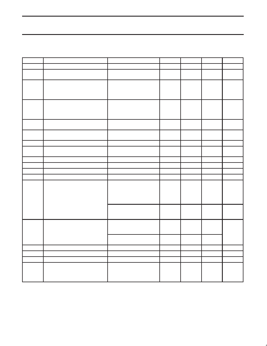
ELECTRICAL CHARACTERISTICS
Tamb = 25 °C, VCC = +5 V to +15 V, unless otherwise specified.
SYMBOL
PARAMETER
TEST CONDITIONS
Min
Typ
Max
UNIT
VCC
Supply voltage
4.5
16
V
ICC
Supply current (low state)1
VCC = 5 V, RL = ∞
6
12
mA
ICC
Su
ly current (low state)
VCC = 15 V, RL = ∞
20
30
mA
Timing error (monostable)
RA = 2k to 100 k
tM
Initial accuracy2
C = 0.1
F
0.75
3.0
%
tM/T
Drift with temperature
T = 1.1 RC
50
150
ppm/
°C
tM/VS
Drift with supply voltage
0.1
0.5
%/V
Timing error (astable)
RA, RB = 1 k to 100 k
tA
Initial accuracy2
C = 0.
F
5
13
%
tA/T
Drift with temperature
VCC = 15 V
400
500
ppm/
°C
tA/VS
Drift with supply voltage
0.3
1
%/V
VC
Control voltage level
VCC = 15 V
9.0
10.0
11.0
V
VC
Control voltage level
VCC = 5 V
2.6
3.33
4.0
V
VTH
Threshold voltage
VCC = 15 V
8.8
10.0
11.2
V
VTH
Threshold voltage
VCC = 5 V
2.4
3.33
4.2
V
ITH
Threshold current3
VCC = 15 V, VTH = 10.5 V
30
250
nA
VTRIG
Trigger voltage
VCC = 15 V
4.5
5.0
5.6
V
VTRIG
Trigger voltage
VCC = 5 V
1.1
1.67
2.2
V
ITRIG
Trigger current
VTRIG = 0 V
0.5
2.0
A
VRESET
Reset voltage5
0.4
0.7
1.0
V
Reset current
VRESET = 0.4 V
0.4
0.1
0.6
mA
IRESET
Reset current
VRESET = 0 V
0.4
1.5
mA
VCC = 15 V
ISINK = 10 mA
0.1
0.25
ISINK = 50 mA
0.4
0.75
V
VO
Output voltage (low)
ISINK = 100 mA
2.0
3.2
VOL
Output voltage (low)
ISINK = 200 mA
2.5
VCC = 5 V
ISINK = 8 mA
0.25
0.3
V
ISINK = 5 mA
0.15
0.25
VCC = 15 V
ISOURCE = 200 mA
12.5
VOH
Output voltage (high)
ISOURCE = 100 mA
12.75
13.3
V
OH
g( g )
VCC = 5 V
ISOURCE = 100 mA
2.75
3.3
tR
Rise time of output
100
300
ns
tF
Fall time of output
100
300
ns
Discharge leakage current
20
100
nA
Matching characteristics4
Initial accuracy2
1.0
2.0
%
Drift with temperature
±10
ppm/
°C
Drift with supply voltage
0.2
0.5
%/V
NOTES:
1. Supply current when output is high is typically 1.0 mA less.
2. Tested at VCC = 5 V and VCC = 15 V.
3. This will determine maximum value of RA+RB. For 15 V operation, the max total R = 10 M, and for 5 V operation, the maximum total
R = 3.4 M
.
4. Matching characteristics refer to the difference between performance characteristics for each timer section in the monostable mode.
5. Specified with trigger input high. In order to guarantee reset the voltage at reset pin must be less than or equal to 0.4 V. To disable reset
function, the voltage at reset pin has to be greater than 1 V.
6. Time measured from a positive-going input pulse from 0 to 0.4 VCC into the threshold to the drop from high to low of the output. Trigger is
tied to threshold.
相關PDF資料 |
PDF描述 |
|---|---|
| 933948930602 | FM, AUDIO DEMODULATOR, PDSO16 |
| 933948930623 | FM, AUDIO DEMODULATOR, PDSO16 |
| 933948970602 | FM, AUDIO SINGLE CHIP RECEIVER, PDSO20 |
| 933948970623 | FM, AUDIO SINGLE CHIP RECEIVER, PDSO20 |
| 935040870112 | FM, AUDIO SINGLE CHIP RECEIVER, PDSO20 |
相關代理商/技術參數 |
參數描述 |
|---|---|
| 933255 | 制造商:ERNI Electronics 功能描述:ERMDE 200 M P2 03.7 A--H 制造商:ERNI Electronics 功能描述:933255 / ERMDE 200 M P2 03.7 A--H / ERMET M |
| 933256 | 制造商:ERNI Electronics 功能描述:ERMDE 200 M P2 03.7 A--H 制造商:ERNI Electronics 功能描述:933256 / ERMDE 200 M P2 03.7 A--H / ERMET M |
| 933257 | 制造商:ERNI Electronics 功能描述:ERMD 88 M P2 03.7 A--H 制造商:ERNI Electronics 功能描述:933257 / ERMD 88 M P2 03.7 A--H / ERMET M |
| 933260 | 制造商:ERNI Electronics 功能描述:Conn Hard Metric M 110 POS 2mm Solder ST Thru-Hole |
| 933261 | 制造商:ERNI Electronics 功能描述:ERMSH F 14.95 0.6 M 制造商:ERNI Electronics 功能描述:933261 / ERMSH F 14.95 0.6 M / ERMET X |
發布緊急采購,3分鐘左右您將得到回復。