- 您現(xiàn)在的位置:買賣IC網(wǎng) > PDF目錄36324 > 933670380112 (NXP SEMICONDUCTORS) 4-CHANNEL, DIFFERENTIAL MULTIPLEXER, PDIP16 PDF資料下載
參數(shù)資料
| 型號: | 933670380112 |
| 廠商: | NXP SEMICONDUCTORS |
| 元件分類: | 多路復(fù)用及模擬開關(guān) |
| 英文描述: | 4-CHANNEL, DIFFERENTIAL MULTIPLEXER, PDIP16 |
| 封裝: | PLASTIC, DIP-16 |
| 文件頁數(shù): | 8/15頁 |
| 文件大小: | 121K |
| 代理商: | 933670380112 |
December 1990
2
Philips Semiconductors
Product specication
Dual 4-channel analog
multiplexer/demultiplexer
74HC/HCT4052
FEATURES
Wide analog input voltage range: ± 5 V.
Low “ON” resistance:
80
(typ.) at VCC VEE = 4.5 V
70
(typ.) at VCC VEE = 6.0 V
60
(typ.) at VCC VEE = 9.0 V
Logic level translation:
to enable 5 V logic to communicate
with
± 5 V analog signals
Typical “break before make” built in
Output capability: non-standard
ICC category: MSI
GENERAL DESCRIPTION
The 74HC/HCT4052 are high-speed Si-gate CMOS
devices and are pin compatible with the “4052” of the
“4000B” series. They are specified in compliance with
JEDEC standard no. 7A.
The 74HC/HCT4052 are dual 4-channel analog
multiplexers/demultiplexers with common select logic.
Each multiplexer has four independent inputs/outputs (nY0
to nY3) and a common input/output (nZ). The common
channel select logics include two digital select inputs (S0
and S1) and an active LOW enable input (E).
With E LOW, one of the four switches is selected (low
impedance ON-state) by S0 and S1. With E HIGH, all
switches are in the high impedance OFF-state,
independent of S0 and S1.
VCC and GND are the supply voltage pins for the digital
control inputs (S0 and S1, and E). The VCC to GND ranges
are 2.0 to 10.0 V for HC and 4.5 to 5.5 V for HCT. The
analog inputs/outputs (nY0 to nY3, and nZ) can swing
between VCC as a positive limit and VEE as a negative limit.
VCC VEE may not exceed 10.0 V.
For operation as a digital multiplexer/demultiplexer, VEE is
connected to GND (typically ground).
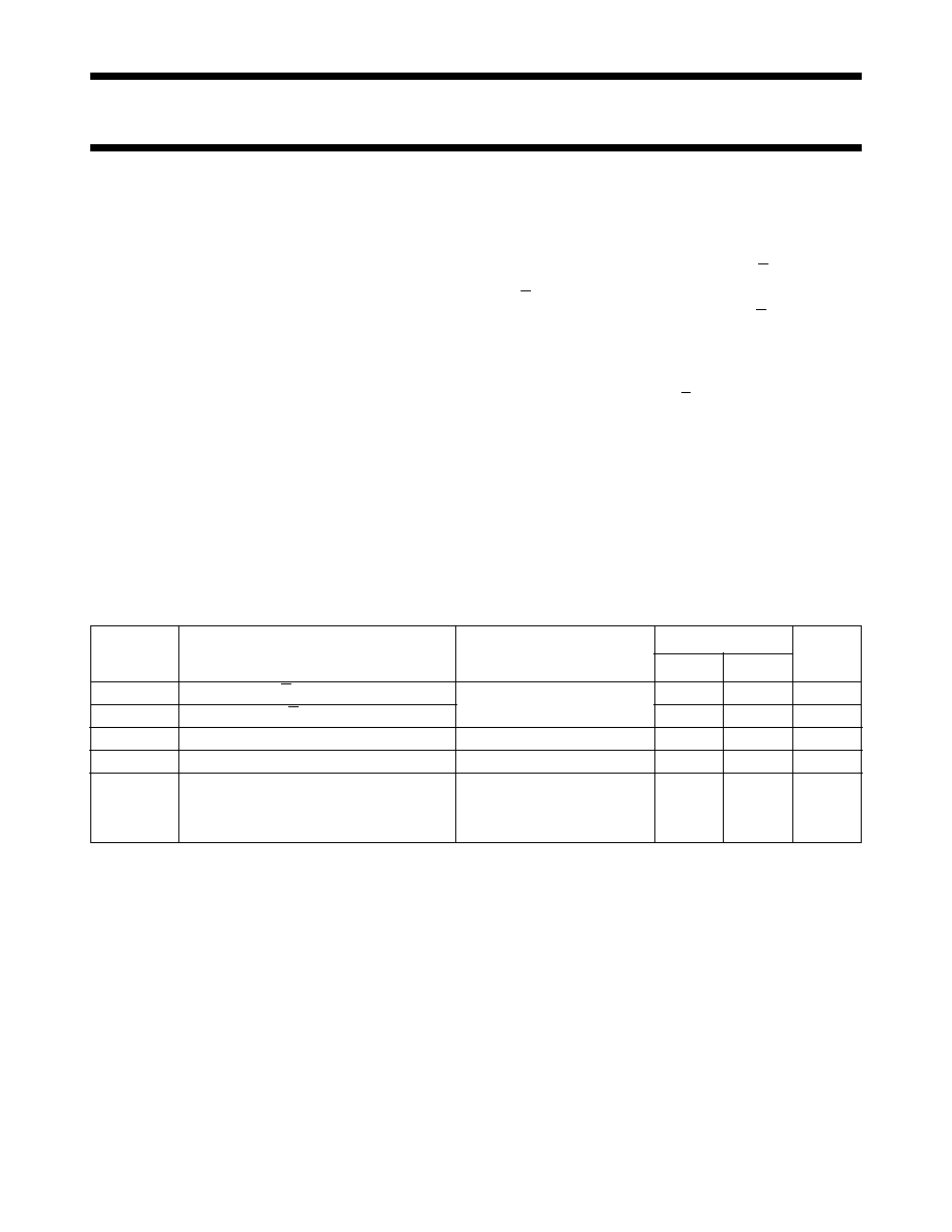
QUICK REFERENCE DATA
VEE = GND = 0 V; Tamb =25 °C; tr =tf = 6 ns
Notes
1. CPD is used to determine the dynamic power dissipation (PD in W):
PD =CPD × VCC2 × fi +∑ {(CL + CS) × VCC2 × fo)} where:
fi = input frequency in MHz
fo = output frequency in MHz
∑ {(CL +CS) × VCC2 × fo)} = sum of outputs
CL = output load capacitance in pF
CS = max. switch capacitance in pF
VCC = supply voltage in V
2. For HC the condition is VI = GND to VCC
For HCT the condition is VI = GND to VCC 1.5 V
SYMBOL
PARAMETER
CONDITIONS
TYPICAL
UNIT
HC
HCT
tPZH/ tPZL
turn “ON” time E or Sn to VOS
CL = 15 pF ; RL =1 k;
VCC =5 V
28
18
ns
tPHZ/ tPLZ
turn “OFF” time E or Sn to VOS
21
13
ns
CI
input capacitance
3.5
pF
CPD
power dissipation capacitance per switch notes 1 and 2
57
pF
CS
max. switch capacitance
independent (Y)
5
pF
common
(Z)
12
pF
相關(guān)PDF資料 |
PDF描述 |
|---|---|
| 935187490118 | 4-CHANNEL, DIFFERENTIAL MULTIPLEXER, PDSO16 |
| 933824730005 | 4-CHANNEL, DIFFERENTIAL MULTIPLEXER, UUC |
| 933714830652 | 4-CHANNEL, DIFFERENTIAL MULTIPLEXER, PDSO16 |
| 933669750652 | 4-CHANNEL, DIFFERENTIAL MULTIPLEXER, PDIP16 |
| 935186930118 | 4-CHANNEL, DIFFERENTIAL MULTIPLEXER, PDSO16 |
相關(guān)代理商/技術(shù)參數(shù) |
參數(shù)描述 |
|---|---|
| 9336CMG | 制造商:Apex Tool Group 功能描述:6 IN. DIAGONAL CUTTING S J PLIERS W/CO-MOLDED GRIPS, LASER HARDENED EDGES, CDD |
| 9336CVN | 制造商:Apex Tool Group 功能描述:6 IN. DIAGONAL CUTTING SOLID JOINT PLIERS, CUSHION GRIP, CARDED |
| 9336N | 制造商:Apex Tool Group 功能描述:6 IN. DIAGONAL CUTTING, GENERAL PURPOSE SOLID JOINT PLIERS |
| 9336-RED | 制造商: 功能描述: 制造商:undefined 功能描述: |
| 9336SCN | 制造商:Apex Tool Group 功能描述:6 IN. DIAGONAL CUTTING SOLID JOINT PLIERS, CUSHION GRIP |
發(fā)布緊急采購,3分鐘左右您將得到回復(fù)。