- 您現在的位置:買賣IC網 > PDF目錄36324 > 933790940112 (NXP SEMICONDUCTORS) TRIPLE 2-CHANNEL, SGL ENDED MULTIPLEXER, PDSO20 PDF資料下載
參數資料
| 型號: | 933790940112 |
| 廠商: | NXP SEMICONDUCTORS |
| 元件分類: | 多路復用及模擬開關 |
| 英文描述: | TRIPLE 2-CHANNEL, SGL ENDED MULTIPLEXER, PDSO20 |
| 封裝: | PLASTIC, SO-20 |
| 文件頁數: | 4/16頁 |
| 文件大小: | 124K |
| 代理商: | 933790940112 |
December 1990
12
Philips Semiconductors
Product specication
Triple 2-channel analog
multiplexer/demultiplexer with latch
74HC/HCT4353
ADDITIONAL AC CHARACTERISTICS FOR 74HC/HCT
Recommended conditions and typical values
GND = 0 V; Tamb =25 °C
Notes to the AC characteristics
1. Adjust input voltage Vis to 0 dBm level (0 dBm = 1 mW into 600 ).
2. Adjust input voltage Vis to 0 dBm level at Vos for 1 MHz (0 dBm = 1 mW into 50 ).
General note
Vis is the input voltage at an nYn or nZ terminal, whichever is assigned as an input.
Vos is the output voltage at an nYn or nZ terminal, whichever is assigned as an output.
SYMBOL
PARAMETER
typ.
UNIT
VCC
(V)
VEE
(V)
Vis(p-p)
(V)
CONDITIONS
sine-wave distortion
f = 1 kHz
0.04
0.02
%
2.25
4.5
2.25
4.5
4.0
8.0
RL = 10 k;CL = 50 pF
(see Fig.14)
sine-wave distortion
f = 10 kHz
0.12
0.06
%
2.25
4.5
2.25
4.5
4.0
8.0
RL = 10 k;CL = 50 pF
(see Fig.14)
switch “OFF” signal
feed-through
50
dB
2.25
4.5
2.25
4.5
note 1
RL = 600 ;CL = 50 pF
f = 1 MHz (see Figs 12 and 15)
crosstalk between
any two switches/
multiplexers
60
dB
2.25
4.5
2.25
4.5
note 1
RL = 600 ;CL = 50 pF;
f = 1 MHz (see Fig.16)
V(pp)
crosstalk voltage between
control and any switch
(peak-to-peak value)
110
220
mV
4.5
0
4.5
RL = 600 ;CL = 50 pF;
f = 1 MHz (E1,E2 or Sn,
square-wave between
VCC and GND, tr =tf = 6 ns)
(see Fig.17)
fmax
minimum frequency response
(
3dB)
160
170
MHz
2.25
4.5
2.25
4.5
note 2
RL =50 ;CL = 10 pF
(see Figs 13 and 14)
CS
maximum switch capacitance
independent (Y)
common (Z)
5
12
pF
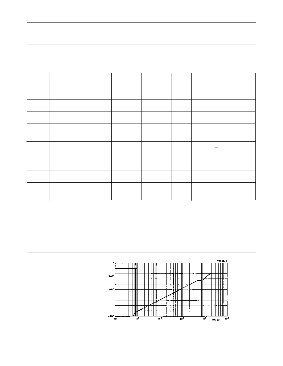
Fig.12 Typical switch “OFF” signal feed-through as a function of frequency.
Test conditions:
VCC = 4.5 V; GND = 0 V; VEE = 4.5 V;
RL =50 ;Rsource =1 k.
相關PDF資料 |
PDF描述 |
|---|---|
| 933835790005 | TRIPLE 2-CHANNEL, SGL ENDED MULTIPLEXER, UUC |
| 933840950602 | SQUARE, TIMER, PDSO8 |
| 933233150602 | SQUARE, TIMER, PDIP8 |
| 933325020602 | SQUARE, TIMER, PDIP8 |
| 935146210025 | SQUARE, TIMER, UUC |
相關代理商/技術參數 |
參數描述 |
|---|---|
| 9337-A17R | 制造商:GC Electronics 功能描述: |
| 9337C | 制造商:Hubbell Premise Wiring 功能描述: |
| 9337-CHR-100 | 制造商:Belden Inc 功能描述: |
| 9337CKE100M | 制造商:RFMD 制造商全稱:RF Micro Devices 功能描述:380W GaN WIDEBAND PULSED |
| 9337CMG | 制造商:Apex Tool Group 功能描述:7 IN. DIAGONAL CUTTING S J PLIERS W/CO-MOLDED GRIPS, LASER HARDENED EDGES, CDD |
發布緊急采購,3分鐘左右您將得到回復。