- 您現在的位置:買賣IC網 > PDF目錄50444 > 934042590115 (NXP SEMICONDUCTORS) 1 A, 600 V, SCR PDF資料下載
參數資料
| 型號: | 934042590115 |
| 廠商: | NXP SEMICONDUCTORS |
| 元件分類: | 晶閘管 |
| 英文描述: | 1 A, 600 V, SCR |
| 封裝: | PLASTIC, SMD, SC-73, 4 PIN |
| 文件頁數: | 1/7頁 |
| 文件大小: | 53K |
| 代理商: | 934042590115 |
Philips Semiconductors
Product specification
Thyristors
BT168GW
logic level for RCD/ GFI/ LCCB applications
GENERAL DESCRIPTION
QUICK REFERENCE DATA
Passivated, sensitive gate thyristor in a plastic
SYMBOL
PARAMETER
MAX.
UNIT
envelope
suitable
for
surface
mounting,
intended for use in Residual Current Devices/
BT168
GW
Ground Fault Interrupters/ Leakage Current
V
DRM, VRRM
Repetitive peak
600
V
Circuit
Breakers
(RCD/ GFI/ LCCB)
I
T(AV)
off-state voltages
applications where a minimum I
GT
limit is
Average on-state
0.6
A
needed. This devices may be interfaced directly
I
T(RMS)
current
to microcontrollers, logic integrated circuits and
I
TSM
RMS on-state current
1
A
other low power gate trigger circuits.
Non-repetitive peak
8
A
on-state current
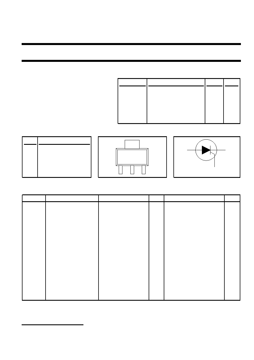
PINNING - SOT223
PIN CONFIGURATION
SYMBOL
PIN
DESCRIPTION
1
cathode
2
anode
3
gate
tab
anode
LIMITING VALUES
Limiting values in accordance with the Absolute Maximum System (IEC 134).
SYMBOL
PARAMETER
CONDITIONS
MIN.
MAX.
UNIT
V
DRM, VRRM
Repetitive peak off-state
-
600
1
V
voltages
I
T(AV)
Average on-state current
half sine wave;
-
0.63
A
T
sp ≤ 112 C
I
T(RMS)
RMS on-state current
all conduction angles
-
1
A
I
TSM
Non-repetitive peak
t = 10 ms
-
8
A
on-state current
t = 8.3 ms
-
9
A
half sine wave;
T
j = 25 C prior to surge
I
2tI2t for fusing
t = 10 ms
-
0.32
A
2s
dI
T/dt
Repetitive rate of rise of
I
TM = 2 A; IG = 10 mA;
-
50
A/
s
on-state current after
dI
G/dt = 100 mA/s
triggering
I
GM
Peak gate current
-
1
A
V
GM
Peak gate voltage
-
5
V
RGM
Peak reverse gate voltage
-
5
V
P
GM
Peak gate power
-
2
W
P
G(AV)
Average gate power
over any 20 ms period
-
0.1
W
T
stg
Storage temperature
-40
150
C
T
j
Operating junction
-
125
C
temperature
ak
g
4
1
23
1 Although not recommended, off-state voltages up to 800V may be applied without damage, but the thyristor may
switch to the on-state. The rate of rise of current should not exceed 15 A/
s.
September 2001
1
Rev 1.000
相關PDF資料 |
PDF描述 |
|---|---|
| 934042910115 | 0.2 A, 2 ELEMENT, SILICON, SIGNAL DIODE |
| 934042920115 | 0.2 A, 2 ELEMENT, SILICON, SIGNAL DIODE |
| 934042890115 | 0.2 A, SILICON, SIGNAL DIODE |
| 934042900115 | 0.2 A, 2 ELEMENT, SILICON, SIGNAL DIODE |
| 934042930115 | 10 V, SILICON, VARIABLE CAPACITANCE DIODE |
相關代理商/技術參數 |
參數描述 |
|---|---|
| 934043060215 | 制造商:NXP Semiconductors 功能描述:TRANSISTOR NPN UHF 50MA SOT23 |
| 934043070215 | 制造商:NXP Semiconductors 功能描述:TRANSISTOR NPN UHF 100MA SOT23 |
| 934043090115 | 制造商:NXP Semiconductors 功能描述:TRANSISTOR SOT-323 制造商:NXP Semiconductors 功能描述:Trans GP BJT NPN 10V 0.1A 3-Pin SC-70 T/R |
| 934044080115 | 制造商:NXP Semiconductors 功能描述:Trans Digital BJT NPN 50V 100mA 3-Pin SC-70 T/R |
| 93405 | 制造商:Harris Corporation 功能描述: |
發布緊急采購,3分鐘左右您將得到回復。