- 您現(xiàn)在的位置:買賣IC網(wǎng) > PDF目錄36324 > 935146210025 (NXP SEMICONDUCTORS) SQUARE, TIMER, UUC PDF資料下載
參數(shù)資料
| 型號: | 935146210025 |
| 廠商: | NXP SEMICONDUCTORS |
| 元件分類: | 模擬波形發(fā)生器 |
| 英文描述: | SQUARE, TIMER, UUC |
| 封裝: | DIE |
| 文件頁數(shù): | 13/15頁 |
| 文件大小: | 188K |
| 代理商: | 935146210025 |
Philips Semiconductors
Product data
NE/SA/SE555/SE555C
Timer
2003 Feb 14
7
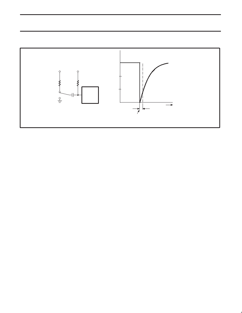
TYPICAL APPLICATIONS
DURATION OF
TRIGGER PULSE AS
SEEN BY THE TIMER
VCC
10 k
2
555
0.001
F
1
SWITCH GROUNDED
AT THIS POINT
0VOLTS
1/3 VCC
VCC
SL00354
Figure 6. AC Coupling of the Trigger Pulse
Trigger Pulse Width Requirements and Time
Delays
Due to the nature of the trigger circuitry, the timer will trigger on the
negative going edge of the input pulse. For the device to time out
properly, it is necessary that the trigger voltage level be returned to
some voltage greater than one third of the supply before the time out
period. This can be achieved by making either the trigger pulse
sufficiently short or by AC coupling into the trigger. By AC coupling
the trigger, see Figure 6, a short negative going pulse is achieved
when the trigger signal goes to ground. AC coupling is most
frequently used in conjunction with a switch or a signal that goes to
ground which initiates the timing cycle. Should the trigger be held
low, without AC coupling, for a longer duration than the timing cycle
the output will remain in a high state for the duration of the low
trigger signal, without regard to the threshold comparator state. This
is due to the predominance of Q15 on the base of Q16, controlling
the state of the bi-stable flip-flop. When the trigger signal then
returns to a high level, the output will fall immediately. Thus, the
output signal will follow the trigger signal in this case.
Another consideration is the “turn-off time”. This is the measurement
of the amount of time required after the threshold reaches 2/3 VCC
to turn the output low. To explain further, Q1 at the threshold input
turns on after reaching 2/3 VCC, which then turns on Q5, which turns
on Q6. Current from Q6 turns on Q16 which turns Q17 off. This
allows current from Q19 to turn on Q20 and Q24 to given an output
low. These steps cause the 2
s max. delay as stated in the data
sheet.
Also, a delay comparable to the turn-off time is the trigger release
time. When the trigger is low, Q10 is on and turns on Q11 which turns
on Q15. Q15 turns off Q16 and allows Q17 to turn on. This turns off
current to Q20 and Q24, which results in output high. When the
trigger is released, Q10 and Q11 shut off, Q15 turns off, Q16 turns on
and the circuit then follows the same path and time delay explained
as “turn off time”. This trigger release time is very important in
designing the trigger pulse width so as not to interfere with the
output signal as explained previously.
相關(guān)PDF資料 |
PDF描述 |
|---|---|
| 933224390602 | SQUARE, TIMER, PDIP8 |
| 933840950623 | SQUARE, TIMER, PDSO8 |
| 933656110623 | SQUARE, TIMER, PDSO8 |
| 933267750602 | SQUARE, TIMER, PDIP8 |
| 933656110602 | SQUARE, TIMER, PDSO8 |
相關(guān)代理商/技術(shù)參數(shù) |
參數(shù)描述 |
|---|---|
| 93515-091000 | 制造商:FCI 功能描述:PCMCIA T2 I/O RECEP 9POS |
| 93515-150000 | 制造商:FCI 功能描述: |
| 93515-250600 | 制造商:FCI 功能描述:PCMCIA T2 I/O RECEP 25POS |
| 93516-PIX | 制造商:FCI 功能描述: |
| 93517-090001 | 制造商:FCI 功能描述:PCMCIA REV CARD FRAME 9P |
發(fā)布緊急采購,3分鐘左右您將得到回復(fù)。