- 您現在的位置:買賣IC網 > PDF目錄36332 > 935260827112 (NXP SEMICONDUCTORS) SPECIALTY CONSUMER CIRCUIT, PDIP32 PDF資料下載
參數資料
| 型號: | 935260827112 |
| 廠商: | NXP SEMICONDUCTORS |
| 元件分類: | 消費家電 |
| 英文描述: | SPECIALTY CONSUMER CIRCUIT, PDIP32 |
| 封裝: | 0.400 INCH, PLASTIC, SOT-232, SDIP-32 |
| 文件頁數: | 5/38頁 |
| 文件大小: | 300K |
| 代理商: | 935260827112 |
第1頁第2頁第3頁第4頁當前第5頁第6頁第7頁第8頁第9頁第10頁第11頁第12頁第13頁第14頁第15頁第16頁第17頁第18頁第19頁第20頁第21頁第22頁第23頁第24頁第25頁第26頁第27頁第28頁第29頁第30頁第31頁第32頁第33頁第34頁第35頁第36頁第37頁第38頁
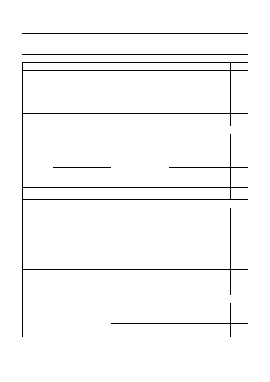
1998 Feb 09
13
Philips Semiconductors
Product specication
Multistandard VIF-PLL with QSS-IF and
AM demodulator
TDA9811
VTOP,19/T
variation of takeover point by
temperature
I19 = 0.4 mA
0.03
0.07
dB/K
I19(sink)
sink current
see Fig.3
no tuner gain reduction;
V19 = 13.2 V
1
A
maximum tuner gain
reduction
1.5
2
2.6
mA
G
IF
IF slip by automatic gain
control
tuner gain current from
20 to 80%
68
dB
AFC circuit (pin 23); see Fig.7 and note 14
S
control steepness
I23/f
note 15
0.5
0.75
1.0
A/kHz
f
IF/T
frequency variation by
temperature
IAFC = 0; note 6
B/G and L standard
±20 × 106 K1
L accent standard
±60 × 106 K1
Vo,23
output voltage upper limit
see Fig.7 without external
components
VP 0.6 VP 0.3
V
output voltage lower limit
0.3
0.6
V
Io,23(source)
output source current
see Fig.7
150
200
250
A
Io,23(sink)
output sink current
150
200
250
A
I
23(p-p)
residual video modulation
current (peak-to-peak value)
B/G and L standard
20
30
A
Sound IF amplier (pins 31 and 32)
Vi SIF(rms)
input signal voltage
sensitivity (RMS value)
FM mode;
3 dB at
intercarrier output pin 20
30
70
V
AM mode;
3 dB at
AF output pin 12
70
100
V
Vi max(rms)
maximum input signal
voltage (RMS value)
FM mode; +1 dB at
intercarrier output pin 20
50
70
mV
AM mode; +1 dB at
AF output pin 12
80
140
mV
GSIFcr
SIF gain control range
FM and AM mode; see Fig.4
60
67
dB
Ri(diff)
differential input resistance
note 2
1.7
2.2
2.7
k
Ci(diff)
differential input capacitance note 2
1.2
1.7
2.5
pF
VI(31,32)
DC input voltage
3.4
V
α
ct(SIF,VIF)
crosstalk attenuation
between SIF and VIF input
between pins 1, 2, 4 and 5
and pins 31 and 32; note 3
50
dB
SIF-AGC detector (pin 8)
I8
charging current
FM mode
8
12
16
A
AM mode
0.8
1.2
1.6
A
discharging current
FM mode
8
12
16
A
normal mode AM
1
1.4
1.8
A
fast mode AM
60
85
110
A
SYMBOL
PARAMETER
CONDITIONS
MIN.
TYP.
MAX.
UNIT
相關PDF資料 |
PDF描述 |
|---|---|
| 935193790112 | SPECIALTY CONSUMER CIRCUIT, PDIP56 |
| 935193810112 | SPECIALTY CONSUMER CIRCUIT, PDIP56 |
| 935224680112 | SPECIALTY CONSUMER CIRCUIT, PDIP56 |
| 935224690112 | SPECIALTY CONSUMER CIRCUIT, PDIP56 |
| 935224700112 | SPECIALTY CONSUMER CIRCUIT, PDIP56 |
相關代理商/技術參數 |
參數描述 |
|---|---|
| 935261069122 | 制造商:NXP Semiconductors 功能描述:IC SECURITY TRANSPONDER PLLMC |
| 935262025112 | 制造商:NXP Semiconductors 功能描述:SUB ONLY IC |
| 935262217118 | 制造商:NXP Semiconductors 功能描述:Real Time Clock Serial 8-Pin SO T/R |
| 935264217557 | 制造商:NXP Semiconductors 功能描述:SUB ONLY IC |
| 935267356112 | 制造商:NXP Semiconductors 功能描述:IC TEA1507PN |
發布緊急采購,3分鐘左右您將得到回復。