- 您現在的位置:買賣IC網 > PDF目錄25564 > 9DB306BL (INTEGRATED DEVICE TECHNOLOGY INC) 9DB SERIES, PLL BASED CLOCK DRIVER, 6 TRUE OUTPUT(S), 0 INVERTED OUTPUT(S), PDSO28 PDF資料下載
參數資料
| 型號: | 9DB306BL |
| 廠商: | INTEGRATED DEVICE TECHNOLOGY INC |
| 元件分類: | 時鐘及定時 |
| 英文描述: | 9DB SERIES, PLL BASED CLOCK DRIVER, 6 TRUE OUTPUT(S), 0 INVERTED OUTPUT(S), PDSO28 |
| 封裝: | 4.40 X 9.70 MM, 0.925 MM HEIGHT, TSSOP-28 |
| 文件頁數: | 1/17頁 |
| 文件大小: | 268K |
| 代理商: | 9DB306BL |
PCI Express Jitter Attenuator
ICS9DB306
DATA SHEET
ICS9DB306BL REVISION C AUGUST 13, 2009
1
2009 Integrated Device Technology, Inc.
GENERAL DESCRIPTION
The ICS9DB306 is a high performance 1-to-6
Differential-to-LVPECL Jitter Attenuator designed for
use in PCI Express systems. In some PCI Express
systems, such as those found in desktop PCs, the
PCI Express clocks are generated from a low
bandwidth, high phase noise PLL frequency synthesizer. In
these systems, a zero delay buffer may be required to attenuate
high frequency random and deterministic jitter components from
the PLL synthesizer and from the system board. The ICS9DB306
has 2 PLL bandwidth modes. In low bandwidth mode, the PLL
loop BW is about 500kHz and this setting will attenuate much of
the jitter from the reference clock input while being high enough
to pass a triangular input spread spectrum profile. There is also
a high bandwidth mode which sets the PLL bandwidth at 1MHz
which will pass more spread spectrum modulation.
For serdes which have x30 reference multipliers instead of x25
multipliers, 5 of the 6 PCI Express outputs (PCIEX1:5) can be
set for 125MHz instead of 100MHz by configuring the appropriate
frequency select pins (FS0:1). Output PCIEX0 will always run at
the reference clock frequency (usually 100MHz) in desktop PC
PCI Express Applications.
FEATURES
Six differential LVPECL output pairs
One differential clock input
CLK and nCLK supports the following input types:
LVPECL, LVDS, LVHSTL, SSTL, HCSL
Maximum output frequency: 140MHz
Input frequency range: 90MHz - 140MHz
VCO range: 450MHz - 700MHz
Output skew: 135ps (maximum)
Cycle-to-Cycle jitter: 30ps (maximum)
RMS phase jitter @ 100MHz, (1.5MHz - 22MHz): 3ps (typical)
3.3V operating supply
0°C to 70°C ambient operating temperature
Available in both standard (RoHS 5) and lead-free (RoHS 6)
packages
Industrial temperature information available upon request
HiPerClockS
ICS
PIN ASSIGNMENT
nOE0
CLK
nCLK
BYPASS
nOE1
PCIEXT0
nPCIEXC0
PCIEXT1
nPCIEXC1
PCIEXT2
nPCIEXC2
PCIEXT3
nPCIEXC3
PCIEXT4
nPCIEXC4
PCIEXT5
nPCIEXC5
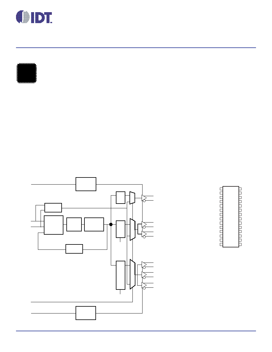
BLOCK DIAGRAM
ICS9DB306
28-Lead TSSOP, 173-MIL
4.4mm x 9.7mm x 0.925mm
body package
L Package
Top View
VEE
PCIEXT1
PCIEXC1
PCIEXT2
PCIEXC2
VCC
nOE0
nOE1
VCC
PCIEXC3
PCIEXT3
PCIEXC4
PCIEXT4
VEE
VCC
PCIEXC0
PCIEXT0
FS0
nCLK
CLK
PLL_BW
VCCA
VEE
BYPASS
FS1
PCIEXT5
PCIEXC5
VCC
ICS9DB306
28-Lead, 209-MIL SSOP
5.3mm x 10.2mm x 1.75mm
body package
F Package
Top View
Phase
Detector
VCO
Loop
Filter
1 Disabled
0 Enabled
1 Disabled
0 Enabled
÷5
0 ÷4
1 ÷5
0 ÷5
1 ÷4
FS0
FS1
Internal Feedback
÷5
0
1
0
1
0
1
Buffer
1
2
3
4
5
6
7
8
9
10
11
12
13
14
28
27
26
25
24
23
22
21
20
19
18
17
16
15
相關PDF資料 |
PDF描述 |
|---|---|
| 9DB401BGLFT | 9DB SERIES, PLL BASED CLOCK DRIVER, 4 TRUE OUTPUT(S), 0 INVERTED OUTPUT(S), PDSO28 |
| 9DB401BFLFT | 9DB SERIES, PLL BASED CLOCK DRIVER, 4 TRUE OUTPUT(S), 0 INVERTED OUTPUT(S), PDSO28 |
| 9DB401CGLFT | 9DB SERIES, PLL BASED CLOCK DRIVER, 4 TRUE OUTPUT(S), 0 INVERTED OUTPUT(S), PDSO28 |
| 9DB401CFLF | 9DB SERIES, PLL BASED CLOCK DRIVER, 4 TRUE OUTPUT(S), 0 INVERTED OUTPUT(S), PDSO28 |
| 9DB403DGILFT | 9DB SERIES, PLL BASED CLOCK DRIVER, 4 TRUE OUTPUT(S), 0 INVERTED OUTPUT(S), PDSO28 |
相關代理商/技術參數 |
參數描述 |
|---|---|
| 9DB306BLI | 制造商:Integrated Device Technology Inc 功能描述:ZERO DLY PLL CLOCK BFFR SGL 28TSSOP - Rail/Tube |
| 9DB306BLILF | 功能描述:IC JITTER ATTENUATOR 28-TSSOP 制造商:idt, integrated device technology inc 系列:- 包裝:管件 零件狀態:過期 PLL:是 主要用途:PCI Express(PCIe) 輸入:HCSL,LVDS,LVHSTL,LVPECL,SSTL 輸出:LVPECL 電路數:1 比率 - 輸入:輸出:1:6 差分 - 輸入:輸出:是/是 頻率 - 最大值:140MHz 電壓 - 電源:2.97 V ~ 3.63 V 工作溫度:-40°C ~ 85°C 安裝類型:表面貼裝 封裝/外殼:28-TSSOP(0.173",4.40mm 寬) 供應商器件封裝:28-TSSOP 標準包裝:50 |
| 9DB306BLILFT | 功能描述:IC JITTER ATTENUATOR 28-TSSOP 制造商:idt, integrated device technology inc 系列:- 包裝:帶卷(TR) 零件狀態:過期 PLL:是 主要用途:PCI Express(PCIe) 輸入:HCSL,LVDS,LVHSTL,LVPECL,SSTL 輸出:LVPECL 電路數:1 比率 - 輸入:輸出:1:6 差分 - 輸入:輸出:是/是 頻率 - 最大值:140MHz 電壓 - 電源:2.97 V ~ 3.63 V 工作溫度:-40°C ~ 85°C 安裝類型:表面貼裝 封裝/外殼:28-TSSOP(0.173",4.40mm 寬) 供應商器件封裝:28-TSSOP 標準包裝:1,000 |
| 9DB306BLIT | 制造商:Integrated Device Technology Inc 功能描述:ZERO DLY PLL CLOCK BFFR SGL 28TSSOP - Rail/Tube |
| 9DB306BLLF | 功能描述:時鐘合成器/抖動清除器 2 LVPECL Output PCI- Express Buffer RoHS:否 制造商:Skyworks Solutions, Inc. 輸出端數量: 輸出電平: 最大輸出頻率: 輸入電平: 最大輸入頻率:6.1 GHz 電源電壓-最大:3.3 V 電源電壓-最小:2.7 V 封裝 / 箱體:TSSOP-28 封裝:Reel |
發布緊急采購,3分鐘左右您將得到回復。