- 您現(xiàn)在的位置:買賣IC網(wǎng) > PDF目錄164971 > A3PN125-Z1VQ100 FPGA, 3072 CLBS, 125000 GATES, PQFP100 PDF資料下載
參數(shù)資料
| 型號: | A3PN125-Z1VQ100 |
| 元件分類: | FPGA |
| 英文描述: | FPGA, 3072 CLBS, 125000 GATES, PQFP100 |
| 封裝: | 14 X 14 MM, 1.20 MM HEIGHT, 0.50 MM PITCH, VQFP-100 |
| 文件頁數(shù): | 28/100頁 |
| 文件大小: | 3284K |
| 代理商: | A3PN125-Z1VQ100 |
第1頁第2頁第3頁第4頁第5頁第6頁第7頁第8頁第9頁第10頁第11頁第12頁第13頁第14頁第15頁第16頁第17頁第18頁第19頁第20頁第21頁第22頁第23頁第24頁第25頁第26頁第27頁當前第28頁第29頁第30頁第31頁第32頁第33頁第34頁第35頁第36頁第37頁第38頁第39頁第40頁第41頁第42頁第43頁第44頁第45頁第46頁第47頁第48頁第49頁第50頁第51頁第52頁第53頁第54頁第55頁第56頁第57頁第58頁第59頁第60頁第61頁第62頁第63頁第64頁第65頁第66頁第67頁第68頁第69頁第70頁第71頁第72頁第73頁第74頁第75頁第76頁第77頁第78頁第79頁第80頁第81頁第82頁第83頁第84頁第85頁第86頁第87頁第88頁第89頁第90頁第91頁第92頁第93頁第94頁第95頁第96頁第97頁第98頁第99頁第100頁
ProASIC3 nano DC and Switching Characteristics
Ad vance v0.2
2-19
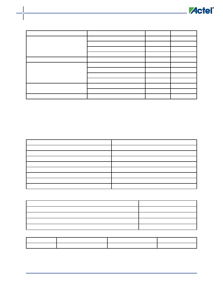
The length of time an I/O can withstand IOSH/IOSL events depends on the junction temperature. The
reliability data below is based on a 3.3 V, 8 mA I/O setting, which is the worst case for this type of
analysis.
For example, at 110°C, the short current condition would have to be sustained for more than three
months to cause a reliability concern. The I/O design does not contain any short circuit protection,
but such protection would only be needed in extremely prolonged stress conditions.
Table 2-23 I/O Short Currents IOSH/IOSL
Drive Strength
IOSL (mA)*
IOSH (mA)*
3.3 V LVTTL / 3.3 V LVCMOS
2 mA
25
27
4 mA
25
27
6 mA
51
54
8 mA
51
54
3.3 V LVCMOS Wide Range
100 A
TBD
2.5 V LVCMOS
2 mA
16
18
4 mA
16
18
6 mA
32
37
8 mA
32
37
1.8 V LVCMOS
2 mA
9
11
4 mA
17
22
1.5 V LVCMOS
2 mA
13
16
* TJ = 100°C
Table 2-24 Duration of Short Circuit Event before Failure
Temperature
Time before Failure
–40°C
> 20 years
–20°C
> 20 years
0°C
> 20 years
25°C
> 20 years
70°C
5 years
85°C
2 years
100°C
6 months
110°C
3 months
Table 2-25 Schmitt Trigger Input Hysteresis
Hysteresis Voltage Value (Typ.) for Schmitt Mode Input Buffers
Input Buffer Configuration
Hysteresis Value (typ.)
3.3 V LVTTL / LVCMOS (Schmitt trigger mode)
240 mV
2.5 V LVCMOS (Schmitt trigger mode)
140 mV
1.8 V LVCMOS (Schmitt trigger mode)
80 mV
1.5 V LVCMOS (Schmitt trigger mode)
60 mV
Table 2-26 I/O Input Rise Time, Fall Time, and Related I/O Reliability
Input Buffer
Input Rise/Fall Time (min.)
Input Rise/Fall Time (max.)
Reliability
LVTTL/LVCMOS
No requirement
10 ns *
20 years (110°C)
* The maximum input rise/fall time is related to the noise induced into the input buffer trace. If the noise is low,
then the rise time and fall time of input buffers can be increased beyond the maximum value. The longer the
rise/fall times, the more susceptible the input signal is to the board noise. Actel recommends signal integrity
evaluation/characterization of the system to ensure that there is no excessive noise coupling into input signals.
相關(guān)PDF資料 |
PDF描述 |
|---|---|
| A3PN125-Z1VQG100I | FPGA, 3072 CLBS, 125000 GATES, PQFP100 |
| A3PN125-Z1VQG100 | FPGA, 3072 CLBS, 125000 GATES, PQFP100 |
| A3PN125-Z2VQ100I | FPGA, 3072 CLBS, 125000 GATES, PQFP100 |
| A3PN125-Z2VQ100 | FPGA, 3072 CLBS, 125000 GATES, PQFP100 |
| A3PN125-Z2VQG100I | FPGA, 3072 CLBS, 125000 GATES, PQFP100 |
相關(guān)代理商/技術(shù)參數(shù) |
參數(shù)描述 |
|---|---|
| A3PN125-Z1VQ100I | 功能描述:IC FPGA NANO 125K GATES 100-VQFP RoHS:否 類別:集成電路 (IC) >> 嵌入式 - FPGA(現(xiàn)場可編程門陣列) 系列:ProASIC3 nano 標準包裝:152 系列:IGLOO PLUS LAB/CLB數(shù):- 邏輯元件/單元數(shù):792 RAM 位總計:- 輸入/輸出數(shù):120 門數(shù):30000 電源電壓:1.14 V ~ 1.575 V 安裝類型:表面貼裝 工作溫度:-40°C ~ 85°C 封裝/外殼:289-TFBGA,CSBGA 供應(yīng)商設(shè)備封裝:289-CSP(14x14) |
| A3PN125-Z1VQG100 | 功能描述:IC FPGA NANO 125K GATES 100-VQFP RoHS:是 類別:集成電路 (IC) >> 嵌入式 - FPGA(現(xiàn)場可編程門陣列) 系列:ProASIC3 nano 標準包裝:152 系列:IGLOO PLUS LAB/CLB數(shù):- 邏輯元件/單元數(shù):792 RAM 位總計:- 輸入/輸出數(shù):120 門數(shù):30000 電源電壓:1.14 V ~ 1.575 V 安裝類型:表面貼裝 工作溫度:-40°C ~ 85°C 封裝/外殼:289-TFBGA,CSBGA 供應(yīng)商設(shè)備封裝:289-CSP(14x14) |
| A3PN125-Z1VQG100I | 功能描述:IC FPGA NANO 125K GATES 100-VQFP RoHS:是 類別:集成電路 (IC) >> 嵌入式 - FPGA(現(xiàn)場可編程門陣列) 系列:ProASIC3 nano 標準包裝:152 系列:IGLOO PLUS LAB/CLB數(shù):- 邏輯元件/單元數(shù):792 RAM 位總計:- 輸入/輸出數(shù):120 門數(shù):30000 電源電壓:1.14 V ~ 1.575 V 安裝類型:表面貼裝 工作溫度:-40°C ~ 85°C 封裝/外殼:289-TFBGA,CSBGA 供應(yīng)商設(shè)備封裝:289-CSP(14x14) |
| A3PN125-Z2VQ100 | 功能描述:IC FPGA NANO 125K GATES 100-VQFP RoHS:否 類別:集成電路 (IC) >> 嵌入式 - FPGA(現(xiàn)場可編程門陣列) 系列:ProASIC3 nano 標準包裝:152 系列:IGLOO PLUS LAB/CLB數(shù):- 邏輯元件/單元數(shù):792 RAM 位總計:- 輸入/輸出數(shù):120 門數(shù):30000 電源電壓:1.14 V ~ 1.575 V 安裝類型:表面貼裝 工作溫度:-40°C ~ 85°C 封裝/外殼:289-TFBGA,CSBGA 供應(yīng)商設(shè)備封裝:289-CSP(14x14) |
| A3PN125-Z2VQ100I | 功能描述:IC FPGA NANO 125K GATES 100-VQFP RoHS:否 類別:集成電路 (IC) >> 嵌入式 - FPGA(現(xiàn)場可編程門陣列) 系列:ProASIC3 nano 標準包裝:152 系列:IGLOO PLUS LAB/CLB數(shù):- 邏輯元件/單元數(shù):792 RAM 位總計:- 輸入/輸出數(shù):120 門數(shù):30000 電源電壓:1.14 V ~ 1.575 V 安裝類型:表面貼裝 工作溫度:-40°C ~ 85°C 封裝/外殼:289-TFBGA,CSBGA 供應(yīng)商設(shè)備封裝:289-CSP(14x14) |
發(fā)布緊急采購,3分鐘左右您將得到回復。