- 您現在的位置:買賣IC網 > PDF目錄164974 > A40MX04-1PL44IX79 FPGA, 547 CLBS, 6000 GATES, 92 MHz, PQCC44 PDF資料下載
參數資料
| 型號: | A40MX04-1PL44IX79 |
| 元件分類: | FPGA |
| 英文描述: | FPGA, 547 CLBS, 6000 GATES, 92 MHz, PQCC44 |
| 封裝: | PLASTIC, LCC-44 |
| 文件頁數: | 99/124頁 |
| 文件大小: | 3142K |
| 代理商: | A40MX04-1PL44IX79 |
第1頁第2頁第3頁第4頁第5頁第6頁第7頁第8頁第9頁第10頁第11頁第12頁第13頁第14頁第15頁第16頁第17頁第18頁第19頁第20頁第21頁第22頁第23頁第24頁第25頁第26頁第27頁第28頁第29頁第30頁第31頁第32頁第33頁第34頁第35頁第36頁第37頁第38頁第39頁第40頁第41頁第42頁第43頁第44頁第45頁第46頁第47頁第48頁第49頁第50頁第51頁第52頁第53頁第54頁第55頁第56頁第57頁第58頁第59頁第60頁第61頁第62頁第63頁第64頁第65頁第66頁第67頁第68頁第69頁第70頁第71頁第72頁第73頁第74頁第75頁第76頁第77頁第78頁第79頁第80頁第81頁第82頁第83頁第84頁第85頁第86頁第87頁第88頁第89頁第90頁第91頁第92頁第93頁第94頁第95頁第96頁第97頁第98頁當前第99頁第100頁第101頁第102頁第103頁第104頁第105頁第106頁第107頁第108頁第109頁第110頁第111頁第112頁第113頁第114頁第115頁第116頁第117頁第118頁第119頁第120頁第121頁第122頁第123頁第124頁
40MX and 42MX FPGA Families
1- 70
v6.1
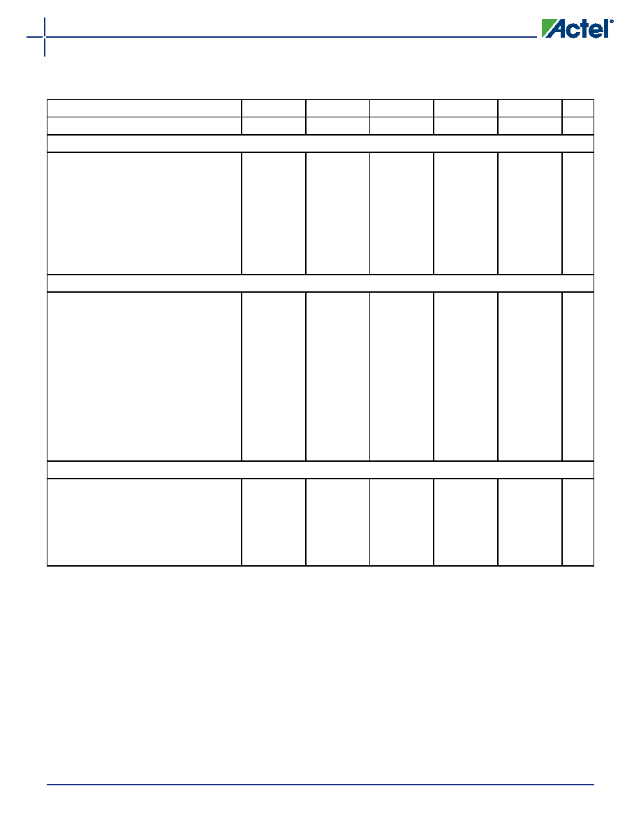
Synchronous SRAM Operations (Continued)
tADH
Address/Data Hold Time
0.0
ns
tRENSU
Read Enable Set-Up
0.6
0.7
0.8
0.9
1.3
ns
tRENH
Read Enable Hold
3.4
3.8
4.3
5.0
7.0
ns
tWENSU
Write Enable Set-Up
2.7
3.0
3.4
4.0
5.6
ns
tWENH
Write Enable Hold
0.0
ns
tBENS
Block Enable Set-Up
2.8
3.1
3.5
4.1
5.7
ns
tBENH
Block Enable Hold
0.0
ns
Asynchronous SRAM Operations
tRPD
Asynchronous Access Time
8.1
9.0
10.2
12.0
16.8
ns
tRDADV
Read Address Valid
8.8
9.8
11.1
13.0
18.2
ns
tADSU
Address/Data Set-Up Time
1.6
1.8
2.0
2.4
3.4
ns
tADH
Address/Data Hold Time
0.0
ns
tRENSUA
Read Enable Set-Up to Address
Valid
0.6
0.7
0.8
0.9
1.3
ns
tRENHA
Read Enable Hold
3.4
3.8
4.3
5.0
7.0
ns
tWENSU
Write Enable Set-Up
2.7
3.0
3.4
4.0
5.6
ns
tWENH
Write Enable Hold
0.0
ns
tDOH
Data Out Hold Time
1.2
1.3
1.5
1.8
2.5
ns
Input Module Propagation Delays
tINPY
Input Data Pad-to-Y
1.0
1.1
1.3
1.5
2.1
ns
tINGO
Input Latch Gate-to-Output
1.4
1.6
1.8
2.1
2.9
ns
tINH
Input Latch Hold
0.0
ns
tINSU
Input Latch Set-Up
0.5
0.6
0.7
1.0
ns
tILA
Latch Active Pulse Width
4.7
5.2
5.9
6.9
9.7
ns
Table 38
A42MX36 Timing Characteristics (Nominal 5.0V Operation)
(Worst-Case Commercial Conditions, VCCA = 4.75V, TJ = 70°C)
‘–3’ Speed
‘–2’ Speed
‘–1’ Speed
‘Std’ Speed
‘–F’ Speed
Parameter Description
Min.
Max.
Min.
Max.
Min.
Max.
Min.
Max.
Min.
Max. Units
Notes:
1. For dual-module macros, use tPD1 + tRD1 + tPDn, tCO + tRD1 + tPDn, or tPD1 + tRD1 + tSUD, whichever is appropriate.
2. Routing delays are for typical designs across worst-case operating conditions. These parameters should be used for estimating
device performance. Post-route timing analysis or simulation is required to determine actual performance.
3. Data applies to macros based on the S-module. Timing parameters for sequential macros constructed from C-modules can be
obtained from the Timer utility.
4. Set-up and hold timing parameters for the Input Buffer Latch are defined with respect to the PAD and the D input. External setup/
hold timing parameters must account for delay from an external PAD signal to the G inputs. Delay from an external PAD signal to
the G input subtracts (adds) to the internal setup (hold) time.
5. Delays based on 35 pF loading.
相關PDF資料 |
PDF描述 |
|---|---|
| A40MX04-1PL44I | FPGA, 547 CLBS, 6000 GATES, 92 MHz, PQCC44 |
| A40MX04-1PL44MX79 | FPGA, 547 CLBS, 6000 GATES, 92 MHz, PQCC44 |
| A40MX04-1PL44M | FPGA, 547 CLBS, 6000 GATES, 92 MHz, PQCC44 |
| A40MX04-1PL44X79 | FPGA, 547 CLBS, 6000 GATES, 92 MHz, PQCC44 |
| A40MX04-1PL44 | FPGA, 547 CLBS, 6000 GATES, 92 MHz, PQCC44 |
相關代理商/技術參數 |
參數描述 |
|---|---|
| A40MX04-1PL44M | 制造商:Microsemi Corporation 功能描述:FPGA 6K GATES 547 CELLS 96MHZ/160MHZ 0.45UM 3.3V/5V 44PLCC - Rail/Tube 制造商:Microsemi Corporation 功能描述:IC FPGA 34 I/O 44PLCC 制造商:Microsemi Corporation 功能描述:IC FPGA MX SGL CHIP 6K 44-PLCC |
| A40MX04-1PL44MX130 | 制造商:Microsemi Corporation 功能描述:FPGA 6K GATES 547 CELLS 96MHZ/160MHZ 0.45UM 3.3V/5V 44PLCC - Rail/Tube |
| A40MX04-1PL44MX3 | 制造商:Microsemi Corporation 功能描述:FPGA 6K GATES 547 CELLS 96MHZ/160MHZ 0.45UM 3.3V/5V 44PLCC - Rail/Tube |
| A40MX04-1PL68 | 功能描述:IC FPGA MX SGL CHIP 6K 68-PLCC RoHS:否 類別:集成電路 (IC) >> 嵌入式 - FPGA(現場可編程門陣列) 系列:MX 標準包裝:90 系列:ProASIC3 LAB/CLB數:- 邏輯元件/單元數:- RAM 位總計:36864 輸入/輸出數:157 門數:250000 電源電壓:1.425 V ~ 1.575 V 安裝類型:表面貼裝 工作溫度:-40°C ~ 125°C 封裝/外殼:256-LBGA 供應商設備封裝:256-FPBGA(17x17) |
| A40MX04-1PL68I | 功能描述:IC FPGA MX SGL CHIP 6K 68-PLCC RoHS:否 類別:集成電路 (IC) >> 嵌入式 - FPGA(現場可編程門陣列) 系列:MX 標準包裝:90 系列:ProASIC3 LAB/CLB數:- 邏輯元件/單元數:- RAM 位總計:36864 輸入/輸出數:157 門數:250000 電源電壓:1.425 V ~ 1.575 V 安裝類型:表面貼裝 工作溫度:-40°C ~ 125°C 封裝/外殼:256-LBGA 供應商設備封裝:256-FPBGA(17x17) |
發布緊急采購,3分鐘左右您將得到回復。