- 您現在的位置:買賣IC網 > PDF目錄22006 > A42MX16-TQG176 (Microsemi SoC)IC FPGA 140I/O 176TQFP PDF資料下載
參數資料
| 型號: | A42MX16-TQG176 |
| 廠商: | Microsemi SoC |
| 文件頁數: | 108/142頁 |
| 文件大小: | 0K |
| 描述: | IC FPGA 140I/O 176TQFP |
| 標準包裝: | 40 |
| 系列: | MX |
| 輸入/輸出數: | 140 |
| 門數: | 24000 |
| 電源電壓: | 3 V ~ 3.6 V,4.75 V ~ 5.25 V |
| 安裝類型: | 表面貼裝 |
| 工作溫度: | 0°C ~ 70°C |
| 封裝/外殼: | 176-LQFP |
| 供應商設備封裝: | 176-TQFP(24x24) |
| 其它名稱: | 1100-1056 |
第1頁第2頁第3頁第4頁第5頁第6頁第7頁第8頁第9頁第10頁第11頁第12頁第13頁第14頁第15頁第16頁第17頁第18頁第19頁第20頁第21頁第22頁第23頁第24頁第25頁第26頁第27頁第28頁第29頁第30頁第31頁第32頁第33頁第34頁第35頁第36頁第37頁第38頁第39頁第40頁第41頁第42頁第43頁第44頁第45頁第46頁第47頁第48頁第49頁第50頁第51頁第52頁第53頁第54頁第55頁第56頁第57頁第58頁第59頁第60頁第61頁第62頁第63頁第64頁第65頁第66頁第67頁第68頁第69頁第70頁第71頁第72頁第73頁第74頁第75頁第76頁第77頁第78頁第79頁第80頁第81頁第82頁第83頁第84頁第85頁第86頁第87頁第88頁第89頁第90頁第91頁第92頁第93頁第94頁第95頁第96頁第97頁第98頁第99頁第100頁第101頁第102頁第103頁第104頁第105頁第106頁第107頁當前第108頁第109頁第110頁第111頁第112頁第113頁第114頁第115頁第116頁第117頁第118頁第119頁第120頁第121頁第122頁第123頁第124頁第125頁第126頁第127頁第128頁第129頁第130頁第131頁第132頁第133頁第134頁第135頁第136頁第137頁第138頁第139頁第140頁第141頁第142頁
40MX and 42MX FPGA Families
1- 64
R e v i sio n 1 1
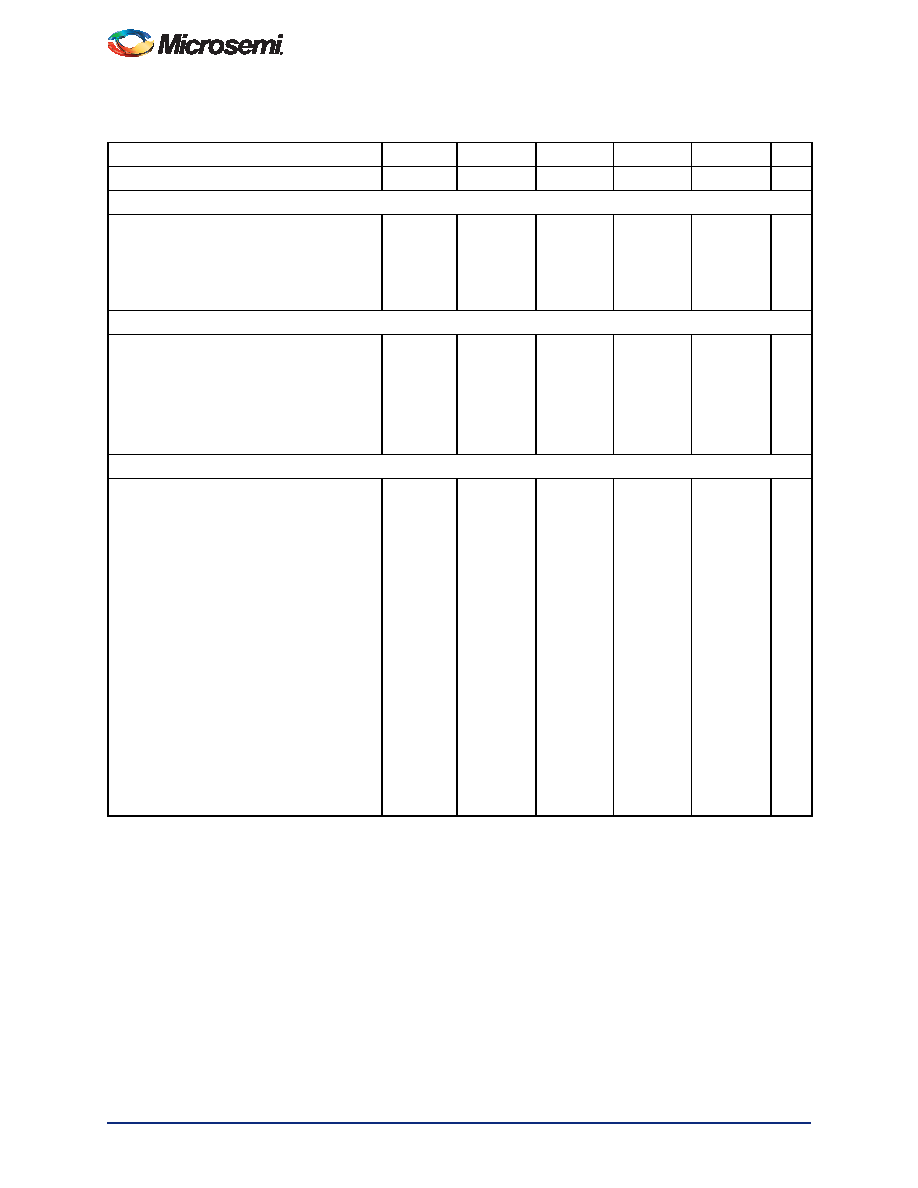
Table 1-35 A42MX16 Timing Characteristics (Nominal 3.3 V Operation)
(Worst-Case Commercial Conditions, VCCA = 3.0 V, TJ = 70°C)
–3 Speed
–2 Speed
–1 Speed
Std Speed
–F Speed
Parameter / Description
Min. Max. Min. Max. Min. Max. Min. Max. Min. Max. Units
Logic Module Propagation Delays1
tPD1
Single Module
1.9
2.1
2.4
2.8
4.0
ns
tCO
Sequential Clock-to-Q
2.0
2.2
2.5
3.0
4.2
ns
tGO
Latch G-to-Q
1.9
2.1
2.4
2.8
4.0
ns
tRS
Flip-Flop (Latch) Reset-to-Q
2.2
2.4
2.8
3.3
4.6
ns
Logic Module Predicted Routing Delays2
tRD1
FO = 1 Routing Delay
1.1
1.2
1.4
1.6
2.3
ns
tRD2
FO = 2 Routing Delay
1.5
1.6
1.8
2.1
3.0
ns
tRD3
FO = 3 Routing Delay
1.8
2.0
2.3
2.7
3.8
ns
tRD4
FO = 4 Routing Delay
2.2
2.4
2.7
3.2
4.5
ns
tRD8
FO = 8 Routing Delay
3.6
4.0
4.5
5.3
7.5
ns
Logic Module Sequential Timing3, 4
tSUD
Flip-Flop (Latch)
Data Input Set-Up
0.5
0.6
0.7
0.9
ns
tHD
Flip-Flop (Latch) Data Input Hold
0.0
ns
tSUENA
Flip-Flop (Latch) Enable Set-Up
1.0
1.1
1.2
1.4
2.0
ns
tHENA
Flip-Flop (Latch) Enable Hold
0.0
ns
tWCLKA
Flip-Flop (Latch)
Clock Active Pulse Width
4.8
5.3
6.0
7.1
9.9
ns
tWASYN
Flip-Flop (Latch)
Asynchronous Pulse Width
6.2
6.9
7.9
9.2
12.9
ns
tA
Flip-Flop Clock Input Period
9.5
10.6
12.0
14.1
19.8
ns
tINH
Input Buffer Latch Hold
0.0
ns
tINSU
Input Buffer Latch Set-Up
0.7
0.8
0.9
1.01
1.4
ns
tOUTH
Output Buffer Latch Hold
0.0
ns
tOUTSU
Output Buffer Latch Set-Up
0.7
0.8
0.89
1.01
1.4
ns
fMAX
Flip-Flop (Latch) Clock Frequency
129
117
108
94
56
MHz
Notes:
1. For dual-module macros use tPD1 + tRD1 + taped, to + tRD1 + taped, or tPD1 + tRD1 + tusk, whichever is appropriate.
2. Routing delays are for typical designs across worst-case operating conditions. These parameters should be used for
estimating device performance. Post-route timing analysis or simulation is required to determine actual performance.
3. Data applies to macros based on the S-module. Timing parameters for sequential macros constructed from C-modules
can be obtained from the Timer utility.
4. Set-up and hold timing parameters for the input buffer latch are defined with respect to the PAD and the D input. External
setup/hold timing parameters must account for delay from an external PAD signal to the G inputs. Delay from an external
PAD signal to the G input subtracts (adds) to the internal setup (hold) time.
5. Delays based on 35 pF loading.
相關PDF資料 |
PDF描述 |
|---|---|
| RMA35DTMT | CONN EDGECARD 70POS R/A .125 SLD |
| EP4CGX30CF23C7N | IC CYCLONE IV FPGA 30K 484-FBGA |
| RSA35DTBT | CONN EDGECARD 70POS R/A .125 SLD |
| EEM25DTKH | CONN EDGECARD 50POS DIP .156 SLD |
| AGL400V5-FG256I | IC FPGA IGLOO 1.5V 256FPBGA |
相關代理商/技術參數 |
參數描述 |
|---|---|
| A42MX16-TQG176A | 功能描述:IC FPGA MX SGL CHIP 24K 176-TQFP RoHS:是 類別:集成電路 (IC) >> 嵌入式 - FPGA(現場可編程門陣列) 系列:MX 標準包裝:40 系列:SX-A LAB/CLB數:6036 邏輯元件/單元數:- RAM 位總計:- 輸入/輸出數:360 門數:108000 電源電壓:2.25 V ~ 5.25 V 安裝類型:表面貼裝 工作溫度:0°C ~ 70°C 封裝/外殼:484-BGA 供應商設備封裝:484-FPBGA(27X27) |
| A42MX16-TQG176I | 功能描述:IC FPGA MX SGL CHIP 24K 176-TQFP RoHS:是 類別:集成電路 (IC) >> 嵌入式 - FPGA(現場可編程門陣列) 系列:MX 標準包裝:40 系列:SX-A LAB/CLB數:6036 邏輯元件/單元數:- RAM 位總計:- 輸入/輸出數:360 門數:108000 電源電壓:2.25 V ~ 5.25 V 安裝類型:表面貼裝 工作溫度:0°C ~ 70°C 封裝/外殼:484-BGA 供應商設備封裝:484-FPBGA(27X27) |
| A42MX16-TQG176M | 制造商:Microsemi Corporation 功能描述:FPGA 24K GATES 608 CELLS 103MHZ/172MHZ 0.45UM 3.3V/5V 176TQF - Trays 制造商:Microsemi Corporation 功能描述:IC FPGA 140 I/O 176TQFP |
| A42MX16-TQG176X288 | 制造商:Microsemi Corporation 功能描述: |
| A42MX16VQ100 | 制造商:Microsemi SOC Products Group 功能描述: |
發布緊急采購,3分鐘左右您將得到回復。