參數資料
| 型號: | AD5066BRUZ |
| 廠商: | Analog Devices Inc |
| 文件頁數: | 1/24頁 |
| 文件大小: | 0K |
| 描述: | IC DAC 16BIT 2.7-5.5V 16TSSOP |
| 標準包裝: | 1 |
| 系列: | nanoDAC™ |
| 設置時間: | 15µs |
| 位數: | 16 |
| 數據接口: | DSP,MICROWIRE?,QSPI?,串行,SPI? |
| 轉換器數目: | 4 |
| 電壓電源: | 單電源 |
| 工作溫度: | -40°C ~ 125°C |
| 安裝類型: | 表面貼裝 |
| 封裝/外殼: | 16-TSSOP(0.173",4.40mm 寬) |
| 供應商設備封裝: | 16-TSSOP |
| 包裝: | 管件 |
| 輸出數目和類型: | 4 電壓,雙極 |
| 采樣率(每秒): | * |
| 產品目錄頁面: | 781 (CN2011-ZH PDF) |
Fully Accurate, 16-Bit, Unbuffered VOUT, Quad SPI
Interface, 2.7 V to 5.5 V nanoDAC in a TSSOP
AD5066
Rev. A
Information furnished by Analog Devices is believed to be accurate and reliable. However, no
responsibilityisassumedbyAnalogDevicesforitsuse,norforanyinfringementsofpatentsorother
rightsofthirdpartiesthatmayresultfromitsuse.Specificationssubjecttochangewithoutnotice.No
license is granted by implication or otherwise under any patent or patent rights of Analog Devices.
Trademarksandregisteredtrademarksarethepropertyoftheirrespectiveowners.
One Technology Way, P.O. Box 9106, Norwood, MA 02062-9106, U.S.A.
Tel: 781.329.4700
Fax: 781.461.3113
2009–2010 Analog Devices, Inc. All rights reserved.
FEATURES
Low power quad 16-bit nanoDAC, ±1 LSB INL
Low total unadjusted error of ±0.1 mV typically
Low zero code error of 0.05 mV typically
Individually buffered reference pins
2.7 V to 5.5 V power supply
Specified over full code range of 0 to 65535
Power-on reset to zero scale or midscale
Per channel power-down with 3 power-down functions
Hardware LDAC with software LDAC override function
CLR
Small 16-lead TSSOP
function to programmable code
APPLICATIONS
Process control
Data acquisition systems
Portable battery-powered instruments
Digital gain and offset adjustment
Programmable voltage and current sources
GENERAL DESCRIPTION
The AD5066 is a low power, 16-bit quad-channel, unbuffered
voltage output nanoDAC offering relative accuracy specifica-
tions of ±1 LSB INL with individual reference pins and can
operate from a single 2.7 V to 5.5 V supply. The AD5066 also
offers a differential accuracy specification of ±1 LSB DNL.
Reference buffers are also provided on-chip. The part uses a
versatile 3-wire, low power Schmitt trigger serial interface that
operates at clock rates up to 50 MHz and is compatible with
standard SPI, QSPI, MICROWIRE, and most DSP interface
standards. The AD5066 incorporates a power-on reset circuit
that ensures the DAC output powers up to zero scale or
midscale and remains there until a valid write to the device
takes place.
Total unadjusted error for the part is <0.8 mV. Zero code error
for the part is 0.05 mV typically.
The AD5066 contains a power-down feature that reduces the
current consumption of the device to typically 400 nA at 5 V
and provides software selectable output loads while in power-
down mode.
The outputs of all DACs can be updated simultaneously using
the hardware LDAC function, with the added functionality of
user software selectable DAC channels to update simultaneously.
There is also an asynchronous CLR that clears all DACs to a
software-selectable code—0 V, midscale, or full scale.
PRODUCT HIGHLIGHTS
1. Quad channel available in 16-lead TSSOP, ±1 LSB INL.
2. Individually buffered voltage reference pins.
3. TUE = ±0.8 mV max and zero code error = 0.1 mV max.
4. High speed serial interface with clock speeds up to 50 MHz.
5. Three power-down modes available to the user.
6. Reset to known output voltage (zero scale or midscale).
Table 1. Related Devices
Part No.
Description
Quad,16-bit buffered DAC,16 LSB INL, TSSOP
Dual,12-/14-/16-bit buffered nanoDAC,
TSSOP
Quad 16-bit nanoDAC, TSSOP
Single, 16-bit nanoDAC, SOT-23
Single, 16-bit nanoDAC, MSOP
Single,16-bit nanoDAC, ±4 LSB INL, SOT-23
14-/16-bit nanoDAC, SOT-23
1 ±1 LSB INL
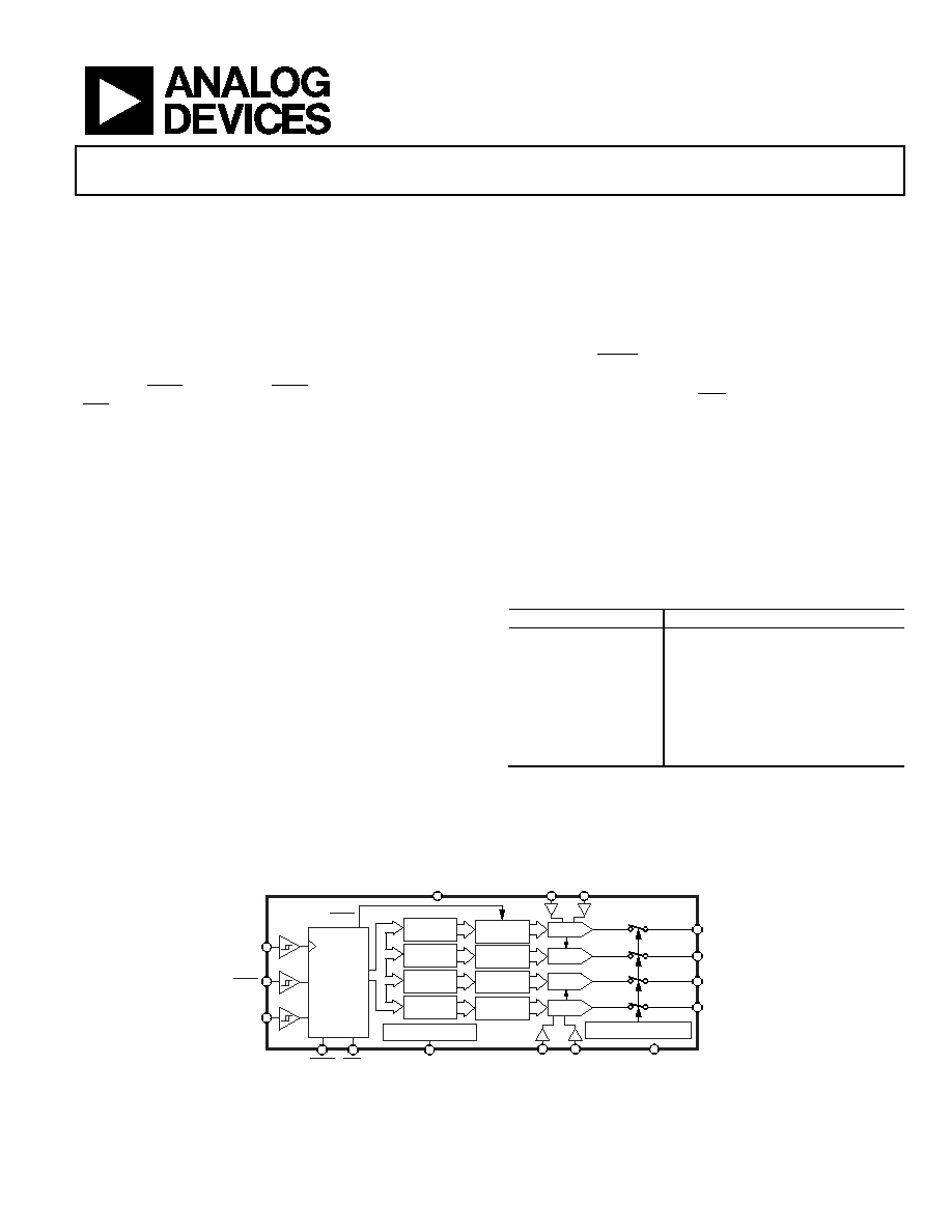
FUNCTIONAL BLOCK DIAGRAM
INTERFACE
LOGIC
INPUT
REGISTER
DIN
LDAC
GND
VDD
LDAC
VREFA
SYNC
SCLK
AD5066
CLR
VOUTA
VOUTB
VOUTC
VOUTD
DAC
REGISTER
DAC A
INPUT
REGISTER
DAC
REGISTER
DAC B
INPUT
REGISTER
DAC
REGISTER
DAC C
DAC D
INPUT
REGISTER
DAC
REGISTER
VREFB
VREFC VREFD
POR
POWER-DOWN LOGIC
POWER-ON RESET
06845-
001
Figure 1.
相關PDF資料 |
PDF描述 |
|---|---|
| VI-21N-MW-F3 | CONVERTER MOD DC/DC 18.5V 100W |
| VI-21N-MW-F2 | CONVERTER MOD DC/DC 18.5V 100W |
| MS3456L32-7S | CONN PLUG 35POS STRAIGHT W/SCKT |
| MS27656T11B13PLC | CONN HSG RCPT 13POS WALL MT PINS |
| LTC1458CG#PBF | IC D/A CONV 12BIT R-R QUAD28SSOP |
相關代理商/技術參數 |
參數描述 |
|---|---|
| AD5066BRUZ-1 | 制造商:AD 制造商全稱:Analog Devices 功能描述:Fully Accurate 16-Bit UnBuffered VOUT DAC SPI Interface 2.7 V to 5.5 V in a TSSOP |
| AD5066BRUZ-1REEL7 | 制造商:AD 制造商全稱:Analog Devices 功能描述:Fully Accurate 16-Bit UnBuffered VOUT DAC SPI Interface 2.7 V to 5.5 V in a TSSOP |
| AD5066BRUZ-REEL7 | 功能描述:IC DAC 16BIT 2.7-5.5V QD 16TSSOP RoHS:是 類別:集成電路 (IC) >> 數據采集 - 數模轉換器 系列:nanoDAC™ 產品培訓模塊:Data Converter Fundamentals DAC Architectures 標準包裝:750 系列:- 設置時間:7µs 位數:16 數據接口:并聯 轉換器數目:1 電壓電源:雙 ± 功率耗散(最大):100mW 工作溫度:0°C ~ 70°C 安裝類型:表面貼裝 封裝/外殼:28-LCC(J 形引線) 供應商設備封裝:28-PLCC(11.51x11.51) 包裝:帶卷 (TR) 輸出數目和類型:1 電壓,單極;1 電壓,雙極 采樣率(每秒):143k |
| AD506ATE/883B | 制造商:Analog 功能描述:Analog Multiplexer 28 PIN CLCC |
| AD506ATE883B | 制造商:Analog 功能描述:Analog Multiplexer 28 PIN CLCC |
發布緊急采購,3分鐘左右您將得到回復。