- 您現在的位置:買賣IC網 > PDF目錄8711 > AD5304BRMZ-REEL7 (Analog Devices Inc)IC DAC 8BIT QUAD VOUT 10-MSOP TR PDF資料下載
參數資料
| 型號: | AD5304BRMZ-REEL7 |
| 廠商: | Analog Devices Inc |
| 文件頁數: | 1/24頁 |
| 文件大小: | 0K |
| 描述: | IC DAC 8BIT QUAD VOUT 10-MSOP TR |
| 產品培訓模塊: | Data Converter Fundamentals DAC Architectures |
| 標準包裝: | 1,000 |
| 設置時間: | 6µs |
| 位數: | 8 |
| 數據接口: | 串行 |
| 轉換器數目: | 4 |
| 電壓電源: | 單電源 |
| 功率耗散(最大): | 4.5W |
| 工作溫度: | -40°C ~ 105°C |
| 安裝類型: | 表面貼裝 |
| 封裝/外殼: | 10-TFSOP,10-MSOP(0.118",3.00mm 寬) |
| 供應商設備封裝: | 10-MSOP |
| 包裝: | 帶卷 (TR) |
| 輸出數目和類型: | 4 電壓,單極;4 電壓,雙極 |
| 采樣率(每秒): | 167k |
2.5 V to 5.5 V, 500 μA, Quad Voltage Output
8-/10-/12-Bit DACs in 10-Lead Packages
Data Sheet
Rev. H
Information furnished by Analog Devices is believed to be accurate and reliable. However, no
responsibilityis assumedbyAnalogDevicesforitsuse,norforanyinfringementsof patentsorother
rightsofthirdpartiesthatmayresultfromitsuse.Specificationssubjecttochangewithoutnotice.No
license is granted by implication or otherwise under any patent or patent rights of Analog Devices.
Trademarksandregisteredtrademarksarethepropertyoftheirrespectiveowners.
One Technology Way, P.O. Box 9106, Norwood, MA 02062-9106, U.S.A.
Tel: 781.329.4700
www.analog.com
Fax: 781.461.3113
2011 Analog Devices, Inc. All rights reserved.
FEATURES
AD5304: 4 buffered 8-Bit DACs in 10-lead MSOP and
10-lead LFCSP
A, W Version: ±1 LSB INL, B Version: ±0.625 LSB INL
AD5314: 4 buffered 10-Bit DACs in 10-lead MSOP and
10-lead LFCSP
A, W Version: ±4 LSB INL, B Version: ±2.5 LSB INL
AD5324: 4 buffered 12-Bit DACs in 10-lead MSOP and
10-lead LFCSP
A, W Version: ±16 LSB INL, B Version: ±10 LSB INL
Low power operation: 500 μA @ 3 V, 600 μA @ 5 V
2.5 V to 5.5 V power supply
Guaranteed monotonic by design over all codes
Power-down to 80 nA @ 3 V, 200 nA @ 5 V
Double-buffered input logic
Output range: 0 V to VREF
Power-on reset to 0 V
Simultaneous update of outputs (LDAC function)
Low power-, SPI-, QSPI-, MICROWIRE-, and DSP-
compatible 3-wire serial interface
On-chip, rail-to-rail output buffer amplifiers
Temperature range 40°C to +105°C
Qualified for automotive applications
APPLICATIONS
Portable battery-powered instruments
Digital gain and offset adjustment
Programmable voltage and current sources
Programmable attenuators
Industrial process controls
GENERAL DESCRIPTION
buffered voltage output DACs in 10-lead MSOP and 10-lead
LFCSP packages that operate from a single 2.5 V to 5.5 V supply,
consuming 500 μA at 3 V. Their on-chip output amplifiers allow
rail-to-rail output swing to be achieved with a slew rate of 0.7 V/μs.
A 3-wire serial interface is used; it operates at clock rates up to
30 MHz and is compatible with standard SPI, QSPI, MICROWIRE,
and DSP interface standards.
The references for the four DACs are derived from one reference
pin. The outputs of all DACs can be updated simultaneously using
the software LDAC function. The parts incorporate a power-on
reset circuit, and ensure that the DAC outputs power up to 0 V
and remains there until a valid write takes place to the device.
The parts contain a power-down feature that reduces the current
consumption of the device to 200 nA @ 5 V (80 nA @ 3 V).
The low power consumption of these parts in normal operation
makes them ideally suited to portable battery-operated equipment.
The power consumption is 3 mW at 5 V, 1.5 mW at 3 V, reducing
to 1 μW in power-down mode.
1 Protected by U.S. Patent No. 5,969,657.
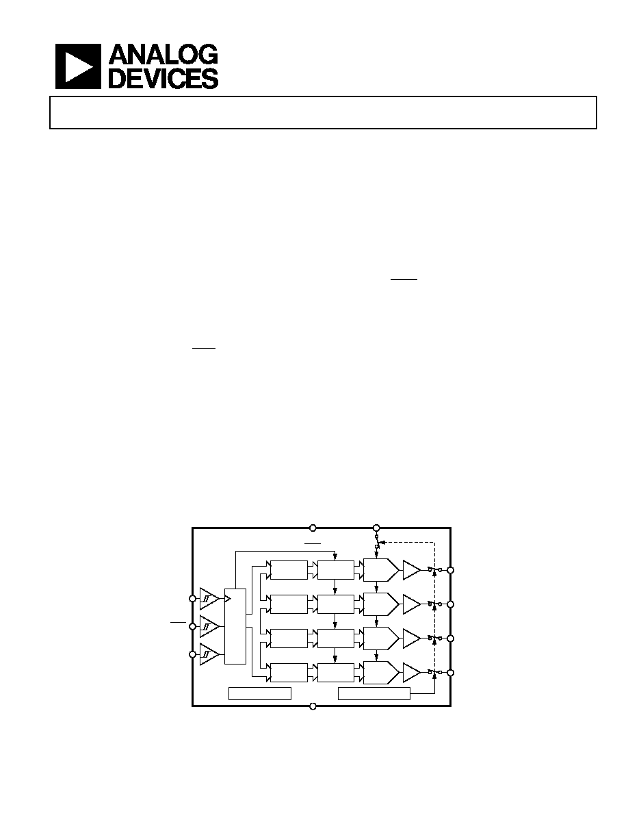
FUNCTIONAL BLOCK DIAGRAM
INPUT
REGISTER
DAC
REGISTER
STRING
DAC A
VOUTA
BUFFER
INPUT
REGISTER
DAC
REGISTER
STRING
DAC B
VOUTB
BUFFER
AD5304/AD5314/AD5324
INPUT
REGISTER
DAC
REGISTER
STRING
DAC C
VOUTC
BUFFER
INPUT
REGISTER
DAC
REGISTER
STRING
DAC D
VOUTD
BUFFER
REFIN
VDD
GND
POWER-DOWN LOGIC
POWER-ON RESET
LDAC
IN
T
E
R
F
A
C
E
LO
GIC
SCLK
SYNC
DIN
00
92
9-
0
01
Figure 1.
相關PDF資料 |
PDF描述 |
|---|---|
| LTC1426CS8 | IC PWM D/A CONV 6BIT DUAL 8-SOIC |
| AD5445YRU-REEL7 | IC DAC 12BIT PAR IOUT 20TSSOP TR |
| VE-B5H-MV-F1 | CONVERTER MOD DC/DC 52V 150W |
| VE-J3H-MY | CONVERTER MOD DC/DC 52V 50W |
| ICS9112AM-26T | IC CLK BUFFER 1:4 133MHZ 8-SOIC |
相關代理商/技術參數 |
參數描述 |
|---|---|
| AD5305 | 制造商:AD 制造商全稱:Analog Devices 功能描述:2.5 V to 5.5 V, 500 uA, Parallel Interface Quad Voltage-Output 8-/10-/12-Bit DACs |
| AD5305_06 | 制造商:AD 制造商全稱:Analog Devices 功能描述:2.5 V to 5.5 V, 500 ??A, 2-Wire Interface Interface |
| AD53052 | 制造商:Analog Devices 功能描述: |
| AD53054KP-REEL | 制造商:Analog Devices 功能描述: |
| AD53054KPZ-RL | 制造商:Analog Devices 功能描述: |
發布緊急采購,3分鐘左右您將得到回復。