- 您現在的位置:買賣IC網 > PDF目錄8742 > AD5312ARMZ-REEL7 (Analog Devices Inc)IC DAC 10BIT DUAL R-R 10-MSOP PDF資料下載
參數資料
| 型號: | AD5312ARMZ-REEL7 |
| 廠商: | Analog Devices Inc |
| 文件頁數: | 1/24頁 |
| 文件大小: | 0K |
| 描述: | IC DAC 10BIT DUAL R-R 10-MSOP |
| 產品培訓模塊: | Data Converter Fundamentals DAC Architectures |
| 標準包裝: | 1,000 |
| 設置時間: | 6µs |
| 位數: | 10 |
| 數據接口: | 串行 |
| 轉換器數目: | 2 |
| 電壓電源: | 單電源 |
| 功率耗散(最大): | 2.5mW |
| 工作溫度: | -40°C ~ 105°C |
| 安裝類型: | 表面貼裝 |
| 封裝/外殼: | 10-TFSOP,10-MSOP(0.118",3.00mm 寬) |
| 供應商設備封裝: | 10-MSOP |
| 包裝: | 帶卷 (TR) |
| 輸出數目和類型: | 2 電壓,單極;2 電壓,雙極 |
| 采樣率(每秒): | 143k |
2.5 V to 5.5 V, 230 μA, Dual Rail-to-Rail,
Voltage Output 8-/10-/12-Bit DACs
AD5302/AD5312/AD5322
Rev. D
Information furnished by Analog Devices is believed to be accurate and reliable. However, no
responsibilityis assumedbyAnalogDevicesforitsuse,norforanyinfringements of patents or other
rightsofthirdpartiesthatmayresultfromitsuse.Specificationssubjecttochangewithoutnotice.No
license is granted by implication or otherwise under any patent or patent rights of Analog Devices.
Trademarksandregisteredtrademarksarethepropertyoftheirrespectiveowners.
One Technology Way, P.O. Box 9106, Norwood, MA 02062-9106, U.S.A.
Tel: 781.329.4700
www.analog.com
Fax: 781.461.3113
2006-2011 Analog Devices, Inc. All rights reserved.
FEATURES
AD5302: Two 8-bit buffered DACs in 1 package
A version: ±1 LSB INL, B version: ±0.5 LSB INL
AD5312: Two 10-bit buffered DACs in 1 package
A version: ±4 LSB INL, B version: ±2 LSB INL
AD5322: Two 12-bit buffered DACs in 1 package
A version: ±16 LSB INL, B version: ±8 LSB INL
10-lead MSOP
Micropower operation: 300 μA @ 5 V (including
reference current)
Power-down to 200 nA @ 5 V, 50 nA @ 3 V
2.5 V to 5.5 V power supply
Double-buffered input logic
Guaranteed monotonic by design over all codes
Buffered/Unbuffered reference input options
0 V to VREF output voltage
Power-on-reset to 0 V
Simultaneous update of DAC outputs via LDAC
Low power serial interface with Schmitt-triggered inputs
On-chip rail-to-rail output buffer amplifiers
Qualified for automotive applications
APPLICATIONS
Portable battery-powered instruments
Digital gain and offset adjustment
Programmable voltage and current sources
Programmable attenuators
GENERAL DESCRIPTION
The AD5302/AD5312/AD5322 are dual 8-, 10-, and 12-bit
buffered voltage output DACs in a 10-lead MSOP that operate
from a single 2.5 V to 5.5 V supply, consuming 230 μA at 3 V.
Their on-chip output amplifiers allow the outputs to swing rail-
to-rail with a slew rate of 0.7 V/μs. The AD5302/AD5312/AD5322
utilize a versatile 3-wire serial interface that operates at clock
rates up to 30 MHz and is compatible with standard SPI,
QSPI, MICROWIRE, and DSP interface standards.
The references for the two DACs are derived from two reference
pins (one per DAC). The reference inputs can be configured as
buffered or unbuffered inputs. The outputs of both DACs can be
updated simultaneously using the asynchronous LDAC input.
The parts incorporate a power-on reset circuit, which ensures
that the DAC outputs power-up to 0 V and remain there until a
valid write takes place to the device. The parts contain a power-
down feature that reduces the current consumption of the
devices to 200 nA at 5 V (50 nA at 3 V) and provides software-
selectable output loads while in power-down mode.
The low power consumption of these parts in normal operation
makes them ideally suited for portable battery-operated
equipment. The power consumption is 1.5 mW at 5 V, 0.7 mW
at 3 V, reducing to 1 μW in power-down mode.
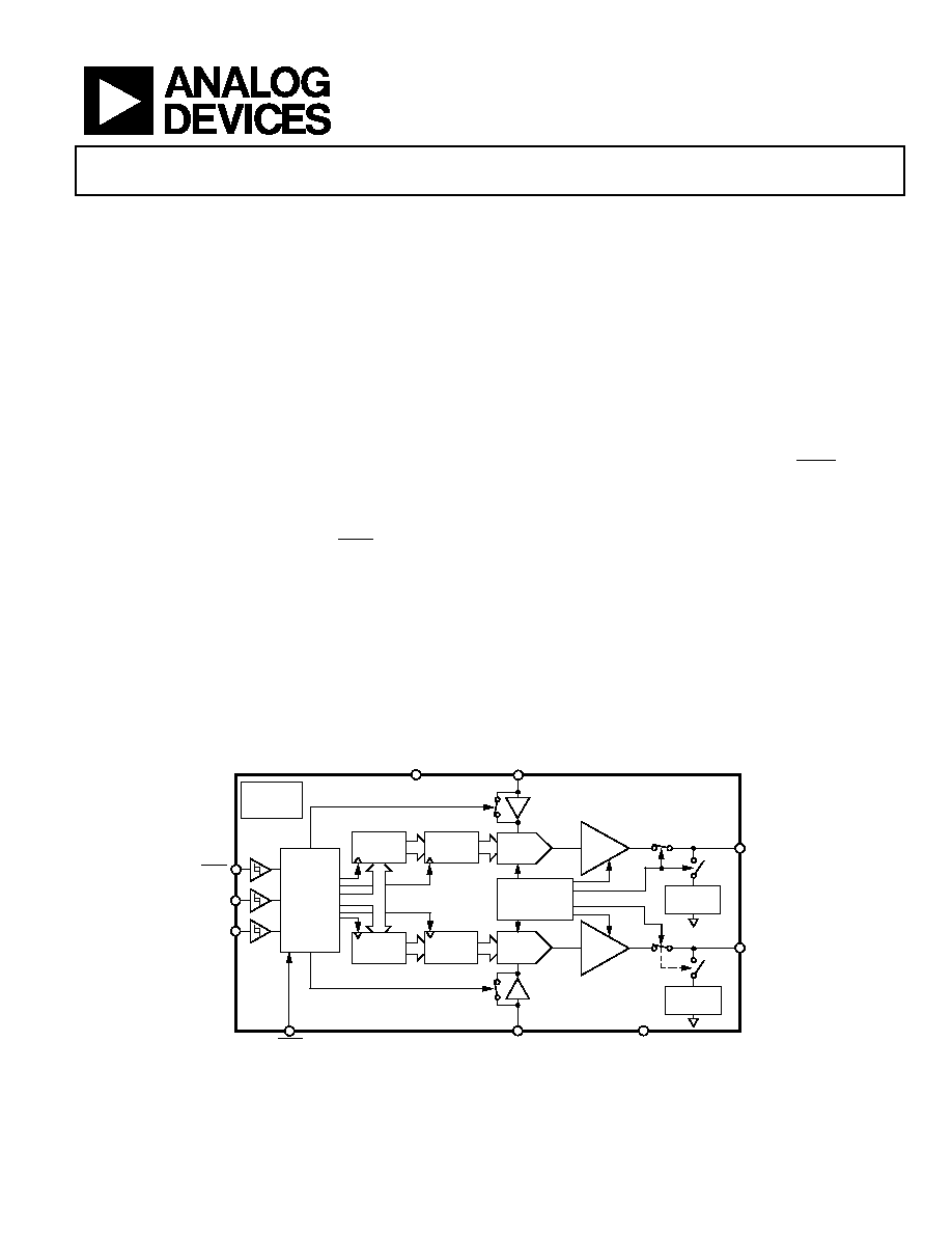
FUNCTIONAL BLOCK DIAGRAM
DAC
REGISTER
RESISTOR
NETWORK
POWER-DOWN
LOGIC
RESISTOR
NETWORK
BUFFER
STRING
DAC
STRING
DAC
AD5302/AD5312/AD5322
INPUT
REGISTER
INPUT
REGISTER
DAC
REGISTER
INTERFACE
LOGIC
SCLK
POWER-ON
RESET
VDD
VREFA
VOUTA
VOUTB
GND
VREFB
LDAC
DIN
00
92
8-
00
1
SYNC
BUFFER
Figure 1.
相關PDF資料 |
PDF描述 |
|---|---|
| VI-21W-MW-F3 | CONVERTER MOD DC/DC 5.5V 100W |
| IDT5V2310PGGI | IC CLK BUFF 1:10 200MHZ 24-TSSOP |
| SI5330B-A00206-GM | IC CLK BUFFER TRANSLA 1:4 24-QFN |
| MPC94551EF | IC CLOCK BUFFER 1:4 160MHZ 8SOIC |
| VI-JNW-MZ-F1 | CONVERTER MOD DC/DC 5.5V 25W |
相關代理商/技術參數 |
參數描述 |
|---|---|
| AD5312BRM | 功能描述:IC DAC 10BIT DUAL R-R OUT 10MSOP RoHS:否 類別:集成電路 (IC) >> 數據采集 - 數模轉換器 系列:- 標準包裝:2,400 系列:- 設置時間:- 位數:18 數據接口:串行 轉換器數目:3 電壓電源:模擬和數字 功率耗散(最大):- 工作溫度:-40°C ~ 85°C 安裝類型:表面貼裝 封裝/外殼:36-TFBGA 供應商設備封裝:36-TFBGA 包裝:帶卷 (TR) 輸出數目和類型:* 采樣率(每秒):* |
| AD5312BRM-REEL | 功能描述:IC DAC 10BIT DUAL W/BUFF 10-MSOP RoHS:否 類別:集成電路 (IC) >> 數據采集 - 數模轉換器 系列:- 標準包裝:2,400 系列:- 設置時間:- 位數:18 數據接口:串行 轉換器數目:3 電壓電源:模擬和數字 功率耗散(最大):- 工作溫度:-40°C ~ 85°C 安裝類型:表面貼裝 封裝/外殼:36-TFBGA 供應商設備封裝:36-TFBGA 包裝:帶卷 (TR) 輸出數目和類型:* 采樣率(每秒):* |
| AD5312BRM-REEL7 | 功能描述:IC DAC 10BIT DUAL W/BUFF 10-MSOP RoHS:否 類別:集成電路 (IC) >> 數據采集 - 數模轉換器 系列:- 產品培訓模塊:LTC263x 12-, 10-, and 8-Bit VOUT DAC Family 特色產品:LTC2636 - Octal 12-/10-/8-Bit SPI VOUT DACs with 10ppm/°C Reference 標準包裝:91 系列:- 設置時間:4µs 位數:10 數據接口:MICROWIRE?,串行,SPI? 轉換器數目:8 電壓電源:單電源 功率耗散(最大):2.7mW 工作溫度:-40°C ~ 85°C 安裝類型:表面貼裝 封裝/外殼:14-WFDFN 裸露焊盤 供應商設備封裝:14-DFN-EP(4x3) 包裝:管件 輸出數目和類型:8 電壓,單極 采樣率(每秒):* |
| AD5312BRMZ | 功能描述:IC DAC 10BIT DUAL R-R 10-MSOP RoHS:是 類別:集成電路 (IC) >> 數據采集 - 數模轉換器 系列:- 產品培訓模塊:Lead (SnPb) Finish for COTS Obsolescence Mitigation Program 標準包裝:50 系列:- 設置時間:4µs 位數:12 數據接口:串行 轉換器數目:2 電壓電源:單電源 功率耗散(最大):- 工作溫度:-40°C ~ 85°C 安裝類型:表面貼裝 封裝/外殼:8-TSSOP,8-MSOP(0.118",3.00mm 寬) 供應商設備封裝:8-uMAX 包裝:管件 輸出數目和類型:2 電壓,單極 采樣率(每秒):* 產品目錄頁面:1398 (CN2011-ZH PDF) |
| AD5312BRMZ-REEL | 功能描述:IC DAC 10BIT DUAL R-R 10-MSOP TR RoHS:是 類別:集成電路 (IC) >> 數據采集 - 數模轉換器 系列:- 產品培訓模塊:LTC263x 12-, 10-, and 8-Bit VOUT DAC Family 特色產品:LTC2636 - Octal 12-/10-/8-Bit SPI VOUT DACs with 10ppm/°C Reference 標準包裝:91 系列:- 設置時間:4µs 位數:10 數據接口:MICROWIRE?,串行,SPI? 轉換器數目:8 電壓電源:單電源 功率耗散(最大):2.7mW 工作溫度:-40°C ~ 85°C 安裝類型:表面貼裝 封裝/外殼:14-WFDFN 裸露焊盤 供應商設備封裝:14-DFN-EP(4x3) 包裝:管件 輸出數目和類型:8 電壓,單極 采樣率(每秒):* |
發布緊急采購,3分鐘左右您將得到回復。