- 您現在的位置:買賣IC網 > PDF目錄8695 > AD5317BRUZ-REEL7 (Analog Devices Inc)IC DAC 10BIT QUAD W/BUFF 16TSSOP PDF資料下載
參數資料
| 型號: | AD5317BRUZ-REEL7 |
| 廠商: | Analog Devices Inc |
| 文件頁數: | 1/28頁 |
| 文件大小: | 0K |
| 描述: | IC DAC 10BIT QUAD W/BUFF 16TSSOP |
| 產品培訓模塊: | Data Converter Fundamentals DAC Architectures |
| 標準包裝: | 1 |
| 設置時間: | 7µs |
| 位數: | 10 |
| 數據接口: | DSP,MICROWIRE?,QSPI?,串行,SPI? |
| 轉換器數目: | 4 |
| 電壓電源: | 單電源 |
| 工作溫度: | -40°C ~ 105°C |
| 安裝類型: | 表面貼裝 |
| 封裝/外殼: | 16-TSSOP(0.173",4.40mm 寬) |
| 供應商設備封裝: | 16-TSSOP |
| 包裝: | 標準包裝 |
| 輸出數目和類型: | 4 電壓,單極;4 電壓,雙極 |
| 采樣率(每秒): | 143k |
| 其它名稱: | AD5317BRUZREEL7DKR |
當前第1頁第2頁第3頁第4頁第5頁第6頁第7頁第8頁第9頁第10頁第11頁第12頁第13頁第14頁第15頁第16頁第17頁第18頁第19頁第20頁第21頁第22頁第23頁第24頁第25頁第26頁第27頁第28頁
2.5 V to 5.5 V, 400 μA, Quad Voltage Output,
8-/10-/12-Bit DACs in 16-Lead TSSOP
AD5307/AD5317/AD5327
Rev. C
Information furnished by Analog Devices is believed to be accurate and reliable. However, no
responsibilityis assumedbyAnalogDevicesforitsuse,norforanyinfringements of patents or other
rightsofthirdpartiesthatmayresultfromitsuse.Specificationssubjecttochangewithoutnotice.No
license is granted by implication or otherwise under any patent or patent rights of Analog Devices.
Trademarksandregisteredtrademarksarethepropertyoftheirrespectiveowners.
One Technology Way, P.O. Box 9106, Norwood, MA 02062-9106, U.S.A.
Tel: 781.329.4700
www.analog.com
Fax: 781.461.3113
2006 Analog Devices, Inc. All rights reserved.
FEATURES
AD5307: 4 buffered 8-bit DACs in 16-lead TSSOP
A version: ±1 LSB INL; B version: ±0.625 LSB INL
AD5317: 4 buffered 10-bit DACs in 16-lead TSSOP
A version: ±4 LSB INL; B version: ±2.5 LSB INL
AD5327: 4 buffered 12-bit DACs in 16-lead TSSOP
A version: ±16 LSB INL; B version: ±10 LSB INL
Low power operation: 400 μA @ 3 V, 500 μA @ 5 V
2.5 V to 5.5 V power supply
Guaranteed monotonic by design over all codes
Power down to 90 nA @ 3 V, 300 nA @ 5 V (LDAC pin)
Double-buffered input logic
Buffered/unbuffered reference input options
Output range: 0 V to VREF or 0 V to 2 VREF
Power-on reset to 0 V
Simultaneous update of outputs (LDAC pin)
Asynchronous clear facility (CLR pin)
Low power, SPI-, QSPI-, MICROWIRE-, and DSP-
compatible 3-wire serial interface
SDO daisy-chaining option
On-chip rail-to-rail output buffer amplifiers
Temperature range of 40°C to +105°C
APPLICATIONS
Portable battery-powered instruments
Digital gain and offset adjustment
Programmable voltage and current sources
Programmable attenuators
Industrial process control
GENERAL DESCRIPTION
The AD5307/AD5317/AD53271 are quad 8-,10-,12-bit buffered
voltage-output DACs in 16-lead TSSOP that operate from single
2.5 V to 5.5 V supplies and consume 400 μA at 3 V. Their on-
chip output amplifiers allow the outputs to swing rail-to-rail with
a slew rate of 0.7 V/μs. The AD5307/AD5317/AD5327 utilize
versatile 3-wire serial interfaces that operate at clock rates up to
30 MHz; these parts are compatible with standard SPI, QSPI,
MICROWIRE, and DSP interface standards.
The references for the four DACs are derived from two reference
pins (one per DAC pair). These reference inputs can be configured
as buffered or unbuffered inputs. Each part incorporates a power-
on reset circuit, ensuring that the DAC outputs power up to 0 V
and remain there until a valid write to the device takes place.
There is also an asynchronous active low CLR pin that clears all
DACs to 0 V. The outputs of all DACs can be updated simul-
taneously using the asynchronous LDAC input. Each part
contains a power-down feature that reduces the current
consumption of the device to 300 nA @ 5 V (90 nA @ 3 V). The
parts can also be used in daisy-chaining applications using the
SDO pin.
All three parts are offered in the same pinout, allowing users to
select the amount of resolution appropriate for their application
without redesigning their circuit board.
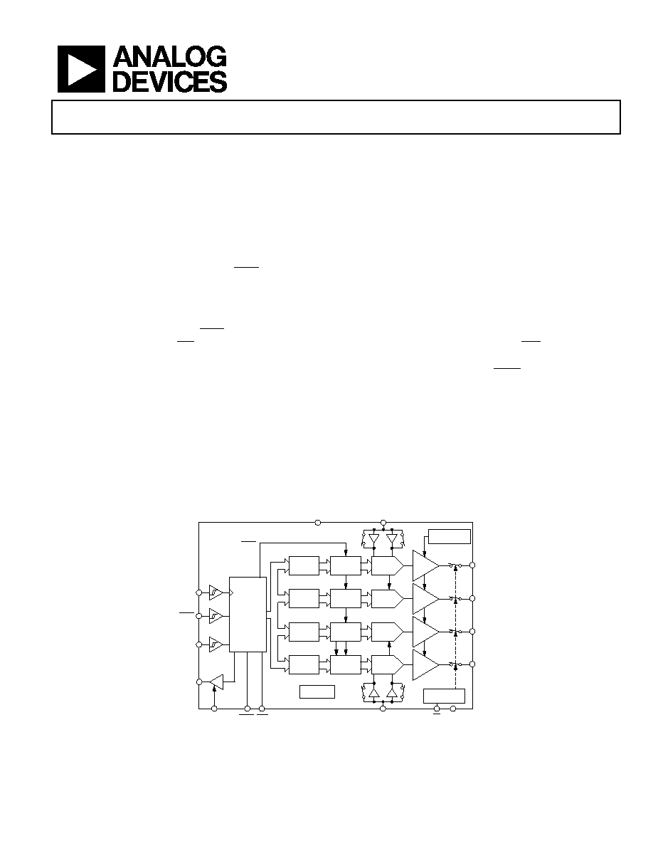
FUNCTIONAL BLOCK DIAGRAM
VDD
VREFAB
VREFCD
POWER-ON
RESET
POWER-DOWN
LOGIC
GND
AD5307/AD5317/AD5327
LDAC
PD
LDAC CLR
DCEN
SDO
DIN
SYNC
SCLK
BUFFER
INPUT
REGISTER
DAC
REGISTER
STRING
DAC D
INPUT
REGISTER
DAC
REGISTER
STRING
DAC C
INPUT
REGISTER
DAC
REGISTER
STRING
DAC B
INPUT
REGISTER
DAC
REGISTER
STRING
DAC A
VOUTD
VOUTC
VOUTB
VOUTA
GAIN-SELECT
LOGIC
INTERFACE
LOGIC
02067-
001
Figure 1.
1 Protected by U.S. Patent No. 5,969,657; other patents pending.
相關PDF資料 |
PDF描述 |
|---|---|
| VI-BN4-MV-F1 | CONVERTER MOD DC/DC 48V 150W |
| VI-BN3-MV-F2 | CONVERTER MOD DC/DC 24V 150W |
| V300A12H400BF2 | CONVERTER MOD DC/DC 12V 400W |
| VI-BN2-MV-F4 | CONVERTER MOD DC/DC 15V 150W |
| AD5415YRUZ-REEL7 | IC DAC 12BIT DUAL MULT 24-TSSOP |
相關代理商/技術參數 |
參數描述 |
|---|---|
| AD5317RBCPZ-RL7 | 制造商:Analog Devices 功能描述: 制造商:Analog Devices 功能描述:10-BIT 4-CH SPI NANODAC+WITH ON CHIP REF - Tape and Reel 制造商:Analog Devices 功能描述:IC DAC 10BIT SPI/SRL 16LFCSP |
| AD5317RBRUZ | 功能描述:數模轉換器- DAC 10-bit 4-ch SPI nanoDAC+with on chip ref RoHS:否 制造商:Texas Instruments 轉換器數量:1 DAC 輸出端數量:1 轉換速率:2 MSPs 分辨率:16 bit 接口類型:QSPI, SPI, Serial (3-Wire, Microwire) 穩定時間:1 us 最大工作溫度:+ 85 C 安裝風格:SMD/SMT 封裝 / 箱體:SOIC-14 封裝:Tube |
| AD5317RBRUZ-RL7 | 功能描述:數模轉換器- DAC IC 10-bit 4-ch SPI w/on chip ref RoHS:否 制造商:Analog Devices 轉換器數量:4 DAC 輸出端數量:4 轉換速率: 分辨率:12 bit 接口類型:Serial (I2C) 穩定時間: 最大工作溫度:+ 105 C 安裝風格: 封裝 / 箱體:TSSOP 封裝:Reel |
| AD5318 | 制造商:AD 制造商全稱:Analog Devices 功能描述:2.5 V to 5.5 V Octal Voltage Output 8-/10-/12-Bit DACs in 16-Lead TSSOP |
| AD5318ARU | 功能描述:IC DAC 10BIT OCTAL W/BUF 16TSSOP RoHS:否 類別:集成電路 (IC) >> 數據采集 - 數模轉換器 系列:- 標準包裝:47 系列:- 設置時間:2µs 位數:14 數據接口:并聯 轉換器數目:1 電壓電源:單電源 功率耗散(最大):55µW 工作溫度:-40°C ~ 85°C 安裝類型:表面貼裝 封裝/外殼:28-SSOP(0.209",5.30mm 寬) 供應商設備封裝:28-SSOP 包裝:管件 輸出數目和類型:1 電流,單極;1 電流,雙極 采樣率(每秒):* |
發布緊急采購,3分鐘左右您將得到回復。